Electronic devices including transparent conductive coatings including carbon nanotubes and nanowire composites, and methods of making the same
- Summary
- Abstract
- Description
- Claims
- Application Information
AI Technical Summary
Benefits of technology
Problems solved by technology
Method used
Image
Examples
Embodiment Construction
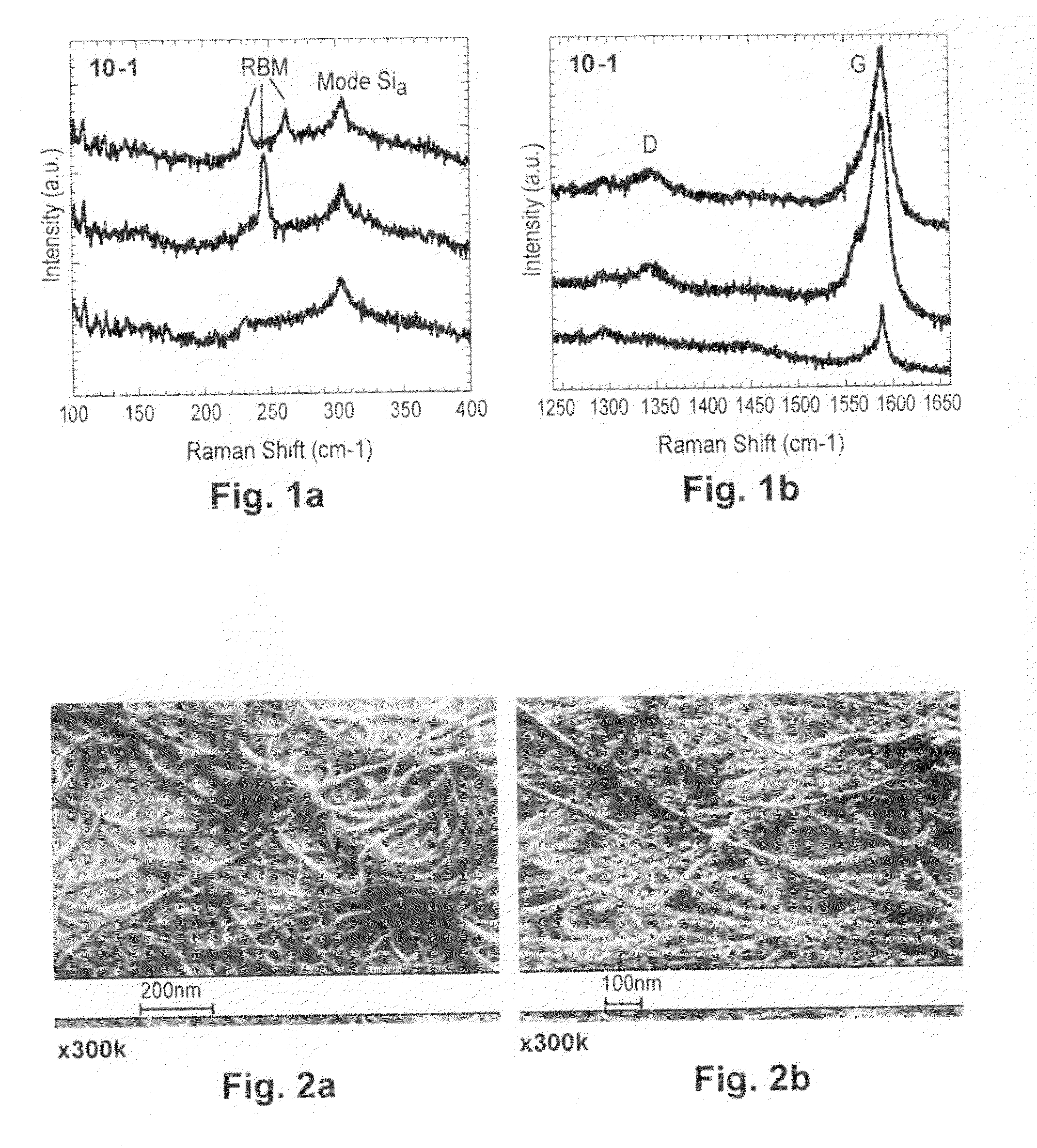
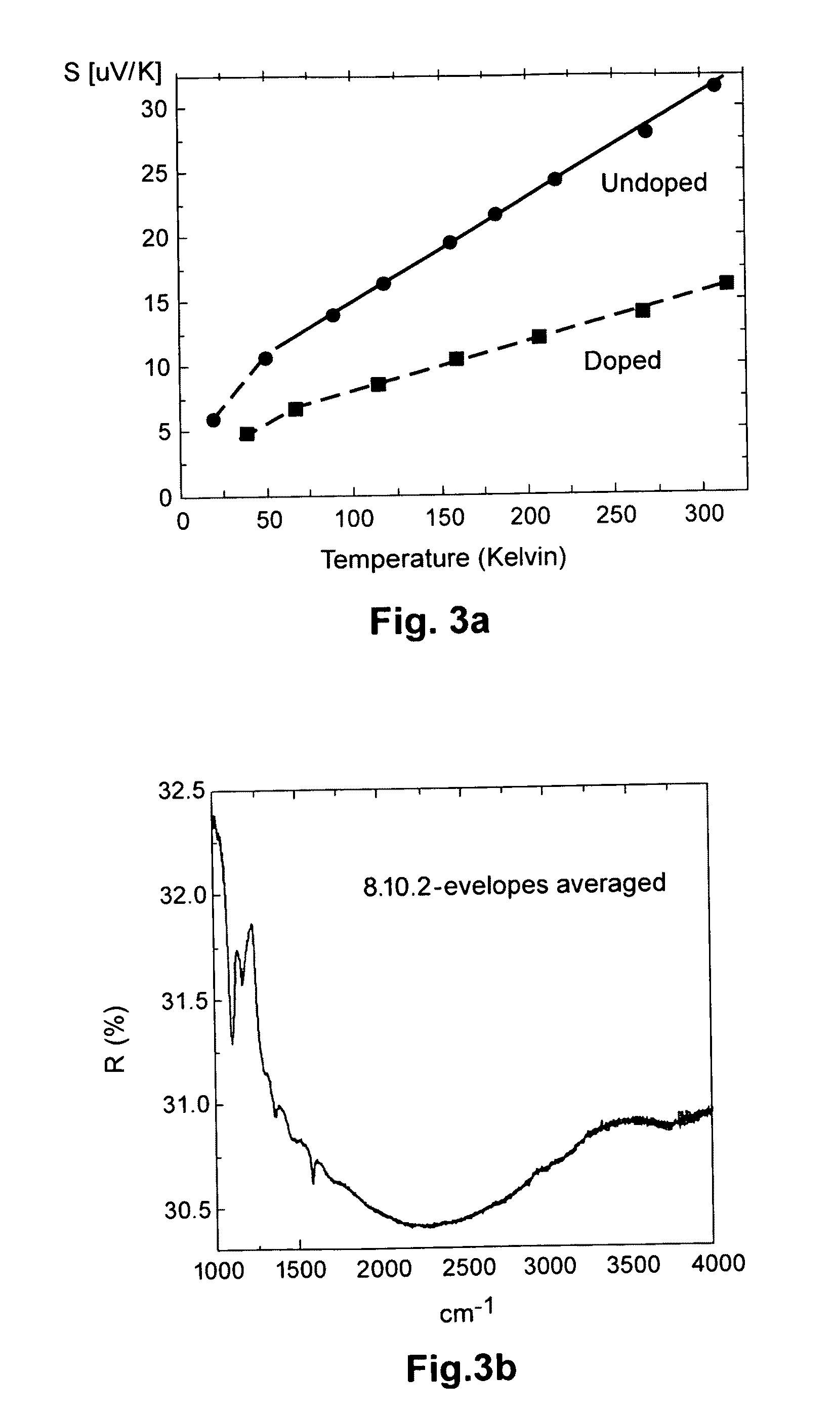
[0034]While thin films made from random meshed networks of carbon nanotubes have been successfully deposited on various transparent substrates, further improvements are necessary before they can be used in photovoltaic devices and other electronic applications such as, for example, OLEDs. Certain example embodiments, however, relate to solution-deposited smooth thin films made from chemically altered double wall nanotubes and composites that have stable sheet resistances below 100 ohms / square at visible transmittance levels of above 83.5%. As described in detail below, the effect of modifying the carbon nanotubes can be verified using thermopower vs. temperature measurements, and changes in optoelectronics properties of the altered films related to weathering may be studied via using SEM, XPS, IR / Raman and spectral transmittance measurements. Certain example embodiments also relate to applications of doped films on glass, namely, capacitive touch sensor electrodes and functional coa...
PUM
| Property | Measurement | Unit |
|---|---|---|
| Fraction | aaaaa | aaaaa |
| Sheet resistance | aaaaa | aaaaa |
| Sheet resistance | aaaaa | aaaaa |
Abstract
Description
Claims
Application Information


