Prevention of oxygen absorption into high-k gate dielectric of silicon-on-insulator based finfet devices

a technology of silicon-on-insulator and high-k gate dielectric, which is applied in the direction of semiconductor devices, electrical equipment, basic electric elements, etc., can solve the problem of limiting the performance of conventional silicon oxide-based gate electrodes

Active Publication Date: 2011-09-08
GLOBALFOUNDRIES US INC
View PDF13 Cites 14 Cited by
  • Summary
  • Abstract
  • Description
  • Claims
  • Application Information

AI Technical Summary

Benefits of technology

[0004]In an exemplary embodiment, a method of forming fin field effect transistor (finFET) devices includes forming a plurality of semiconductor fins over a buried oxide (BOX) layer; performing a nitrogen implant so as to formed nitrided regions in a upper portion of the BOX layer corresponding to regions between the plurality of semiconductor fins; forming a gate dielectric layer over the semiconductor fins and the nitrided regions of the upper portion of the BOX layer; and forming one or more gate electrode materials over the gate dielectric layer; wherein the presence of the nitrided regions of upper portion of the BOX layer prevents oxygen absorption into the gate dielectric layer as a result of thermal processing.

Problems solved by technology

High gate leakage current of nitrided silicon dioxide and the depletion effect of polysilicon gate electrodes limit the performance of conventional silicon oxide-based gate electrodes.

Method used


Image

  • Prevention of oxygen absorption into high-k gate dielectric of silicon-on-insulator based finfet devices
  • Prevention of oxygen absorption into high-k gate dielectric of silicon-on-insulator based finfet devices
  • Prevention of oxygen absorption into high-k gate dielectric of silicon-on-insulator based finfet devices

Examples


Embodiment Construction

over the fin structures, and nitride regions in the upper portions of the BOX layer; and

[0012]FIGS. 8 and 9 illustrate one or more gate electrode materials formed over the high-k dielectric layer so as to define a gate electrode layer for finFET devices.

DETAILED DESCRIPTION

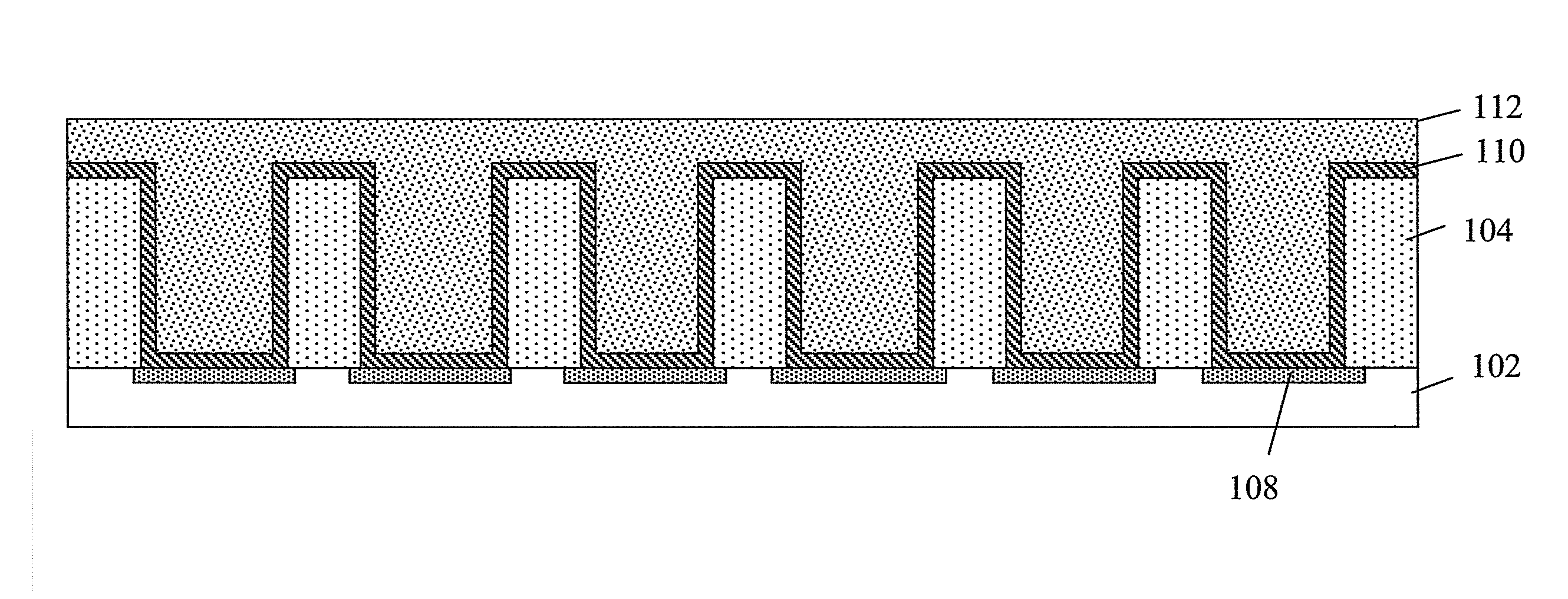
[0013]In current SOI-based finFET devices, the gate dielectric layer is in direct contact with the buried oxide layer (e.g., SiO2) below the semiconductor fins. However, it has been discovered that high-k metal gate (HKMG) exposure to oxygen rich materials may cause severe threshold shift and / or regrowth issues. Because threshold voltage stability and the elimination of gate dielectric regrowth are important parameters for good device operation, it is desirable to be able to eliminate voltage shift or regrowth caused by oxygen rich materials beneath the high-k gate dielectric layer.

[0014]Accordingly, disclosed herein is a structure and method of prevention of oxygen absorption into high-k gate dielectric of silico...


PUM


Abstract

A method of forming fin field effect transistor (finFET) devices includes forming a plurality of semiconductor fins over a buried oxide (BOX) layer; performing a nitrogen implant so as to formed nitrided regions in a upper portion of the BOX layer corresponding to regions between the plurality of semiconductor fins; forming a gate dielectric layer over the semiconductor fins and the nitrided regions of the upper portion of the BOX layer; and forming one or more gate electrode materials over the gate dielectric layer; wherein the presence of the nitrided regions of upper portion of the BOX layer prevents oxygen absorption into the gate dielectric layer as a result of thermal processing.

Description

BACKGROUND[0001]The present invention relates generally to semiconductor device manufacturing and, more particularly, to preventing oxygen absorption into high-k gate dielectric layers of silicon-on-insulator (SOI) based finFET devices.[0002]Fin field effect transistor (finFET) technology is an emerging technology that provides solutions to metal oxide semiconductor FET (MOSFET) scaling problems at and below the 45 nanometer (nm) node. A finFET is a MOSFET that is formed on a semiconductor fin. For example, a finFET includes at least one narrow (e.g., <10 nm wide) semiconductor fin gated on at least two opposing sides of the fin. FinFET structures are advantageously formed on a semiconductor (e.g., silicon)-on-insulator (SOI) substrate, because of the precise control of the fin height, which is determined by the substrate silicon thickness, as well as the ease of electrical isolation by shallow trench isolation structures.[0003]Another area of advancing technology that provides e...

Claims


Application Information

Patent Timeline
Patent Type & Authority Applications(United States)
IPC IPC(8): H01L27/12H01L21/762
CPCH01L27/12H01L21/762H01L29/66795H01L29/785
Inventor GUO, DECHAOKWON, UNOHYEH, CHUN-CHENZHANG, ZHEN
Owner GLOBALFOUNDRIES US INC
Why Eureka
Try Eureka