Variable gain amplifier and high-frequency signal receiving apparatus comprising the same

a gain amplifier and high-frequency signal technology, applied in the direction of amplifier combinations, gain control, gated amplifiers, etc., can solve the problems of consuming more electric power, degrading linearity at low-voltage operation, and unable to receive lossless signals from antennas

Active Publication Date: 2011-09-15
PANASONIC CORP
View PDF7 Cites 25 Cited by
  • Summary
  • Abstract
  • Description
  • Claims
  • Application Information

AI Technical Summary

Benefits of technology

[0015]According to these configurations, the input impedance of the variable gain amplifier can be reduced to a desired value, so that impedance matching is easily performed with the antenna, the signal transmission line, or the like. Furthermore, even when one cascode amplification unit is switched to another, the input impedance of the variable gain amplifier can be kept at a desired value.

Problems solved by technology

As a result, linearity is degraded at a low voltage operation.
Signals from the antenna cannot be received losslessly.
This means that more electric power is consumed.
Also, in conventional variable gain amplifiers, due to their configurations, as the number of cascode amplifiers increases, the parasitic capacitance becomes larger at the signal output end.
Therefore, a larger number of cascode amplifiers significantly degrade frequency characteristics.

Method used


Image

  • Variable gain amplifier and high-frequency signal receiving apparatus comprising the same
  • Variable gain amplifier and high-frequency signal receiving apparatus comprising the same
  • Variable gain amplifier and high-frequency signal receiving apparatus comprising the same

Examples


first embodiment

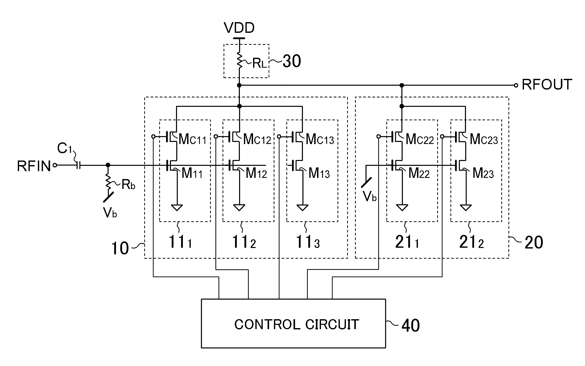
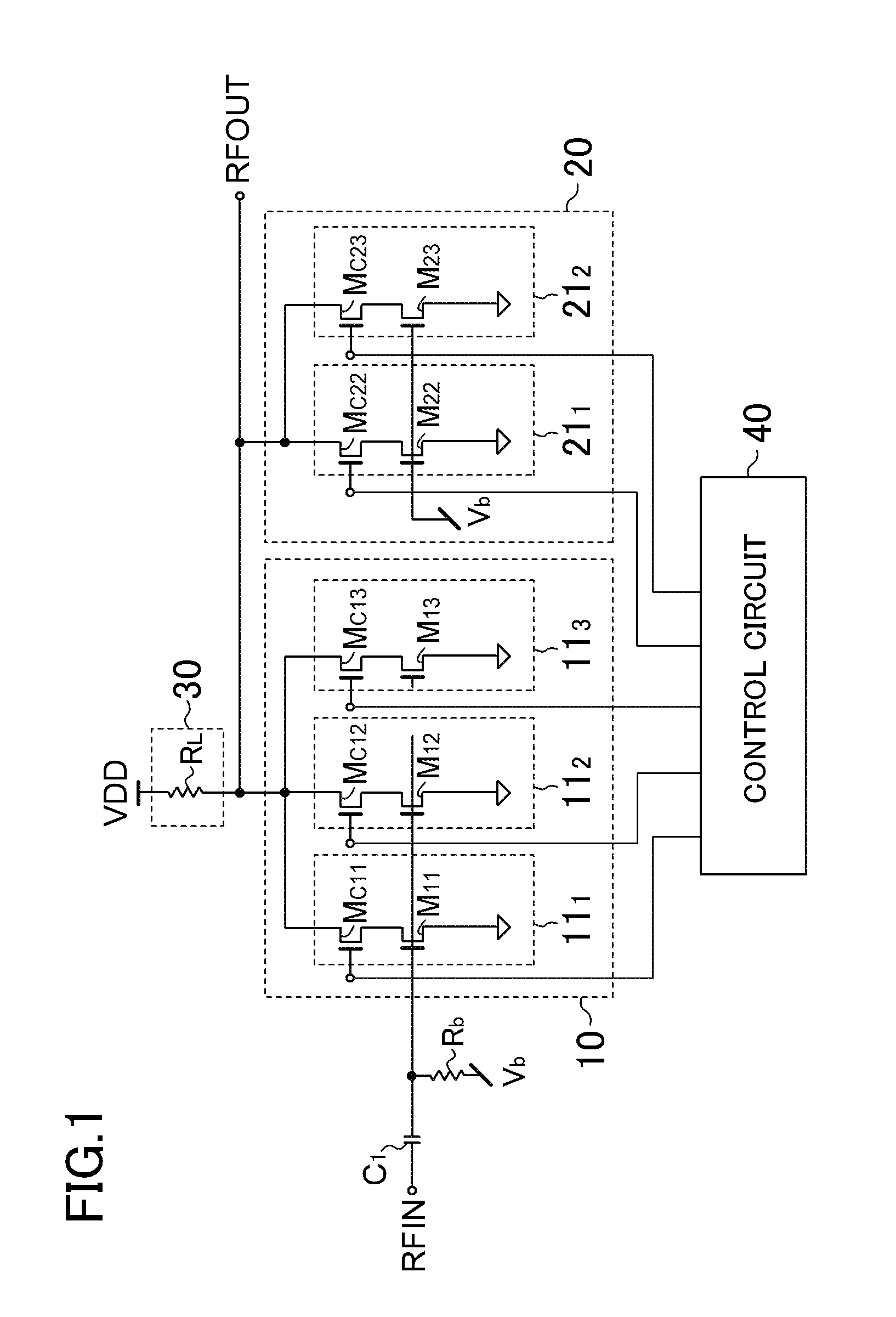
[0023]FIG. 1 is a configuration diagram illustrating a variable gain amplifier according to the first embodiment. A cascode amplification unit 10 includes three cascode amplifiers 11n (n denotes an integer from 1 to 3) connected in parallel. Each cascode amplifier 11n includes an NMOS transistor M1n and an NMOS cascode transistor MC1n. The input end of the cascode amplification unit 10 is connected to the signal input end RFIN of the variable gain amplifier through a DC-cut capacitor C1. A bias voltage Vb is applied to the gate of each transistor M1n through a bias resistor Rb. The size ratio of the transistor M12 to the transistor M13, and the size ratio of the cascode transistor MC12 to the cascode transistor MC13 are each 2:1, where each transistor size is defined by channel width / channel length.

[0024]A cascode current source unit 20 includes two cascode current sources 21m (m denotes an integer from 2 or 3) connected in parallel. Each cascode current source 21m includes an NMOS ...

second embodiment

[0031]Variable gain amplifiers have to receive a signal as losslessly as possible regardless of the intensity of the signal inputted from the antenna. Therefore, the input impedance of a variable gain amplifier preferably has the same value as the characteristic impedance of the antenna (typically, 50Ω or 75Ω for TV receiver).

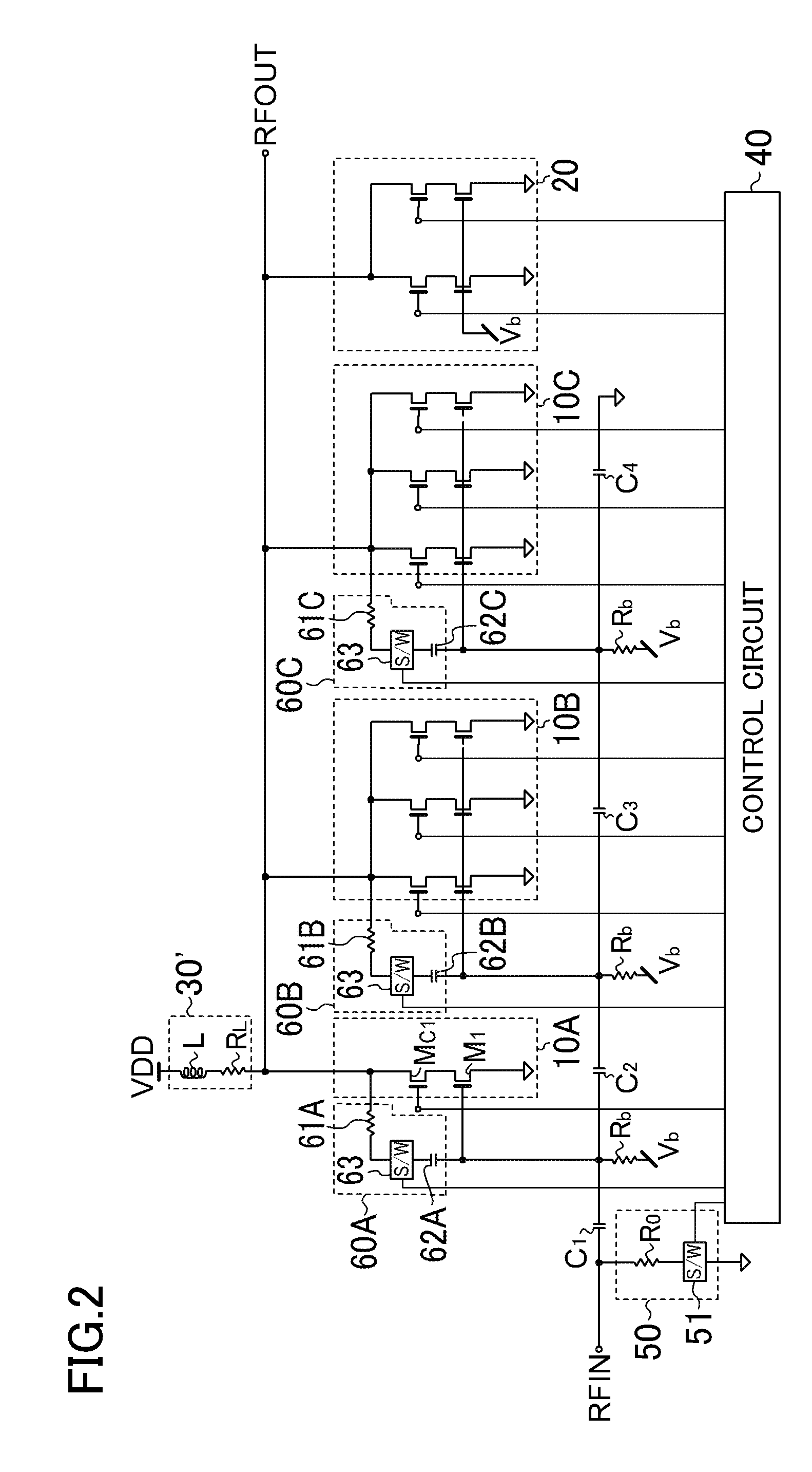
[0032]FIG. 2 is a configuration diagram illustrating a variable gain amplifier according to a second embodiment. The variable gain amplifier according to the second embodiment is configured so that the variations in input impedance at the time of gain switching are smaller. Hereinafter, a description is given only for the parts different from the corresponding parts in the first embodiment.

[0033]The variable gain amplifier according to the second embodiment includes three cascode amplification units 10A, 10B, and 10C. The cascode amplification units 10B and 10C has the same configuration as the cascode amplification unit 10 illustrated in FIG. 1. The cascode am...

third embodiment

[0050]In a CMOS structure, there is a large parasitic capacitance between a capacitor and the silicon substrate. Therefore, the resistance component of the substrate degrades the S / N characteristics of a high-frequency signal. Specifically, in the case where the DC-cut capacitor C1 illustrated in FIG. 2 is provided within the integrated circuit, the noise factor is degraded during maximum gain operation. Therefore, the DC-cut capacitor C1 is preferably provided outside the integrated circuit.

[0051]FIG. 4 illustrates a configuration of a variable gain amplifier according to a third embodiment. In the variable gain amplifier according to the third embodiment, the configuration elements of the variable gain amplifier illustrated in FIG. 2 except the DC-cut capacitor C1 are provided in an integrated circuit 100, and the DC-cut capacitor C1 is provided outside the integrated circuit 100. The DC-cut capacitor C1 may be provided on a printed board, in a module, or in a package.

[0052]In the...


PUM


Abstract

A cascode amplification unit includes a plurality of cascode amplifiers connected in parallel. Each of the cascode amplifiers has two transistors. A cascode current source unit includes a plurality of cascode current sources connected in parallel. Each of the cascode current sources has two transistors. Both the output end of the cascode amplification unit and the output end of the cascode current source unit are connected to a load circuit. The control circuit turns on and off each cascode transistor of the cascode amplifier and each cascode transistor of the cascode current source so that an amount of current passing through the load circuit is constant.

Description

CROSS-REFERENCE TO RELATED APPLICATION[0001]This is a continuation of PCT International Application PCT / JP2009 / 002526 filed on Jun. 4, 2009, which claims priority to Japanese Patent Application No. 2009-004945 filed on Jan. 13, 2009. The disclosures of these applications including the specifications, the drawings, and the claims are hereby incorporated by reference in their entirety.BACKGROUND[0002]The present disclosure relates to a variable gain amplifier used for a wireless communication system, or the like, capable of amplifying a received signal with a desired gain.[0003]In recent years, mobile phones offer not only a verbal communication function, but also wireless communication functions such as digital television, FM radio, Bluetooth (registered trademark), wireless LAN, and GPS. In order to meet the requirements of the miniaturization and price reduction of wireless communication devices and modules included therein, high-performance circuit systems which have not been inte...

Claims


Application Information

Patent Timeline
Patent Type & Authority Applications(United States)
IPC IPC(8): H03G3/00H03F1/22
CPCH03F1/223H03F3/72H03G3/3068H03G1/0029
Inventor KIM, RYANGSUHAYASHI, GEORGE
Owner PANASONIC CORP
Why Eureka
Try Eureka