Method for manufacturing composite substrate comprising wide bandgap semiconductor layer

a semiconductor layer and composite substrate technology, applied in the direction of semiconductor devices, electrical equipment, basic electric elements, etc., can solve the problems of high-performance lasers, difficult to apply gan to power semiconductors, and large defects in deposited gan, so as to prevent cracks or chips of bonded wafers, the effect of cost reduction

Active Publication Date: 2011-09-22
SHIN ETSU CHEM IND CO LTD
View PDF5 Cites 23 Cited by
  • Summary
  • Abstract
  • Description
  • Claims
  • Application Information

AI Technical Summary

Benefits of technology

[0014]The present invention allows the interface of the ion-implanted layer formed in the wide bandgap semiconductor substrate to be subjected to effective and efficient embrittlement without depending on a mechanical impact, and allows bulk crystals of the wide bandgap semiconductor to be transferred onto a handle substrate as thinly as possible, and thus allows the cost to be reduced. In addition, the present invention can also prevent the crack or chip of the bonded wafer, detachment at the bonded surfaces etc. from being caused by a difference in coefficient of thermal expansion between the wide bandgap semiconductor substrate and the handle substrate.BRIEF EXPLANATION OF DRAWINGS
[0015]FIG. 1 is a diagram illustrating an embodiment of a method for manufacturing a bonded wafer according to the present invention.
[0016]FIG. 2 is a diagram illustrating another embodiment of a method for manufacturing a bonded wafer according to the present invention.DESCRIPTION OF REFERENCE SYMBOLS

Problems solved by technology

However, while GaN is deposited by heteroepitaxial growth on single crystalline sapphire or single crystalline SiC as an example, the deposited GaN has a lot of defects due to a difference in lattice constant, and it is now difficult to apply the GaN to power semiconductor, high-performance lasers, etc.
However, the crystal growth takes time, and the crystal is therefore priced extremely high, and now has failed to have a wide range of application.
However, in practice, due to a difference in coefficient of thermal expansion between the donor substrate and the handle substrate (for example, silicon, quartz, sapphire, etc.), it is to be anticipated that simply bonding the both substrates and raising the temperature will cause the substrates to be cracked, thereby failing to form the composite substrate.
However, the film transfer relies on a mechanical method (an impact or the like) so that there is a problem that the substrate is destroyed during the transfer of film from the thin semiconductor substrate with a small diameter due to the insufficient mechanical strength of the substrate.

Method used


Image

  • Method for manufacturing composite substrate comprising wide bandgap semiconductor layer
  • Method for manufacturing composite substrate comprising wide bandgap semiconductor layer
  • Method for manufacturing composite substrate comprising wide bandgap semiconductor layer

Examples


example 1

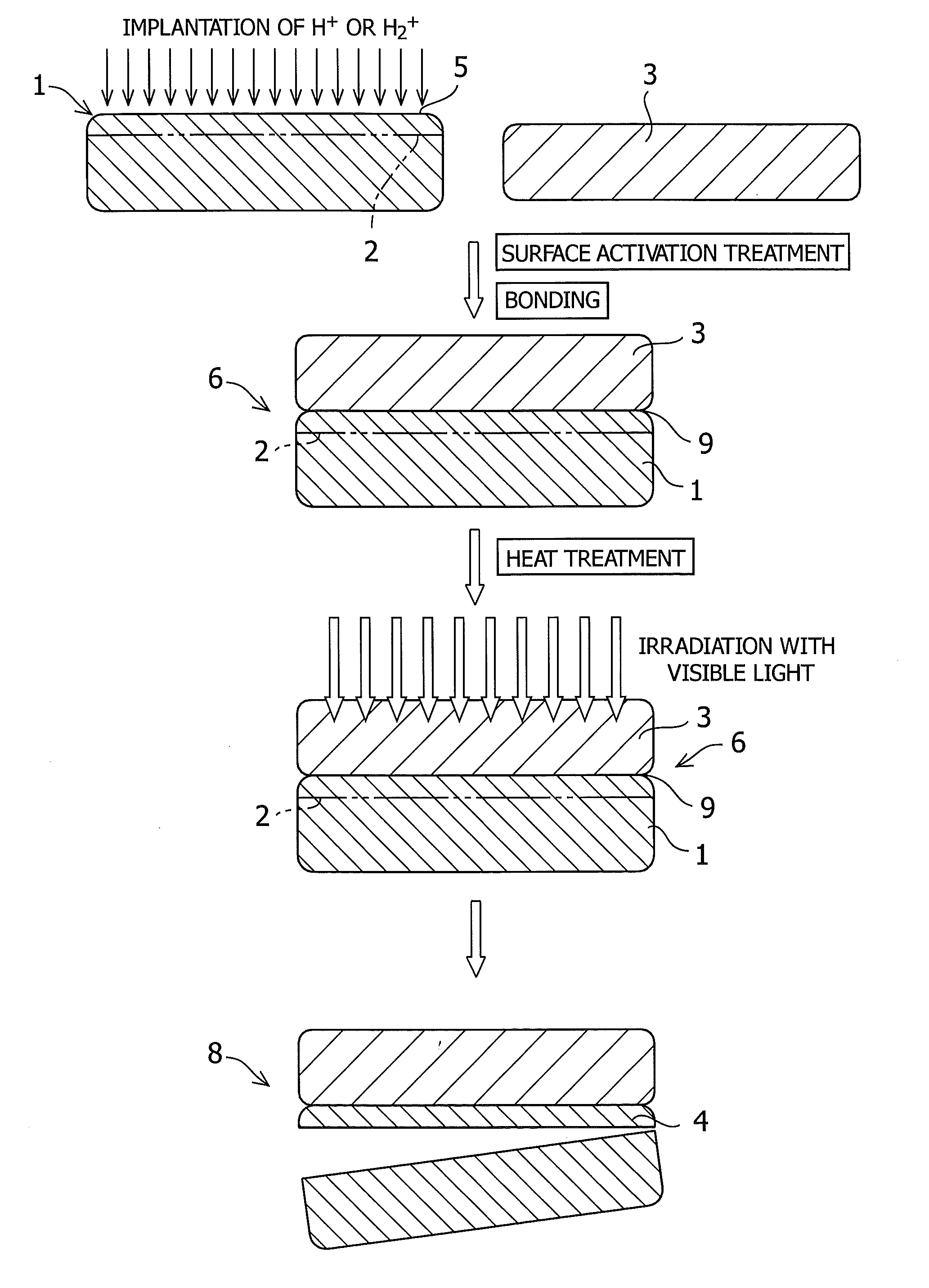
[0071]Implantation of H2+ ions into a GaN substrate of 50 mm in diameter was carried out in a dose amount of 1.35×10¹⁷ atoms / cm2 at an accelerating voltage of 75 KeV. Subsequently, a silicon substrate of 50 mm in diameter to serve as a handle substrate was prepared, and the both substrates were subjected to an ozone water treatment, a UV ozone treatment, an ion beam treatment, or a plasma activation treatment. The substrates were bonded to each other at room temperature, subjected to a heat treatment at 250° C. for 24 hours, and then irradiation with a laser of 532 nm from the transparent GaN substrate side. The irradiation energy was about 0.5 J / cm2. After the irradiation, the application of a light mechanical impact to the bonded surfaces succeeded in transfer of a film of the GaN onto the silicon substrate. The thickness of the GaN transferred in this case was 290 nm.

[0072]This has revealed that the quality of the film transferred is independent of the type of the activation.

example 2

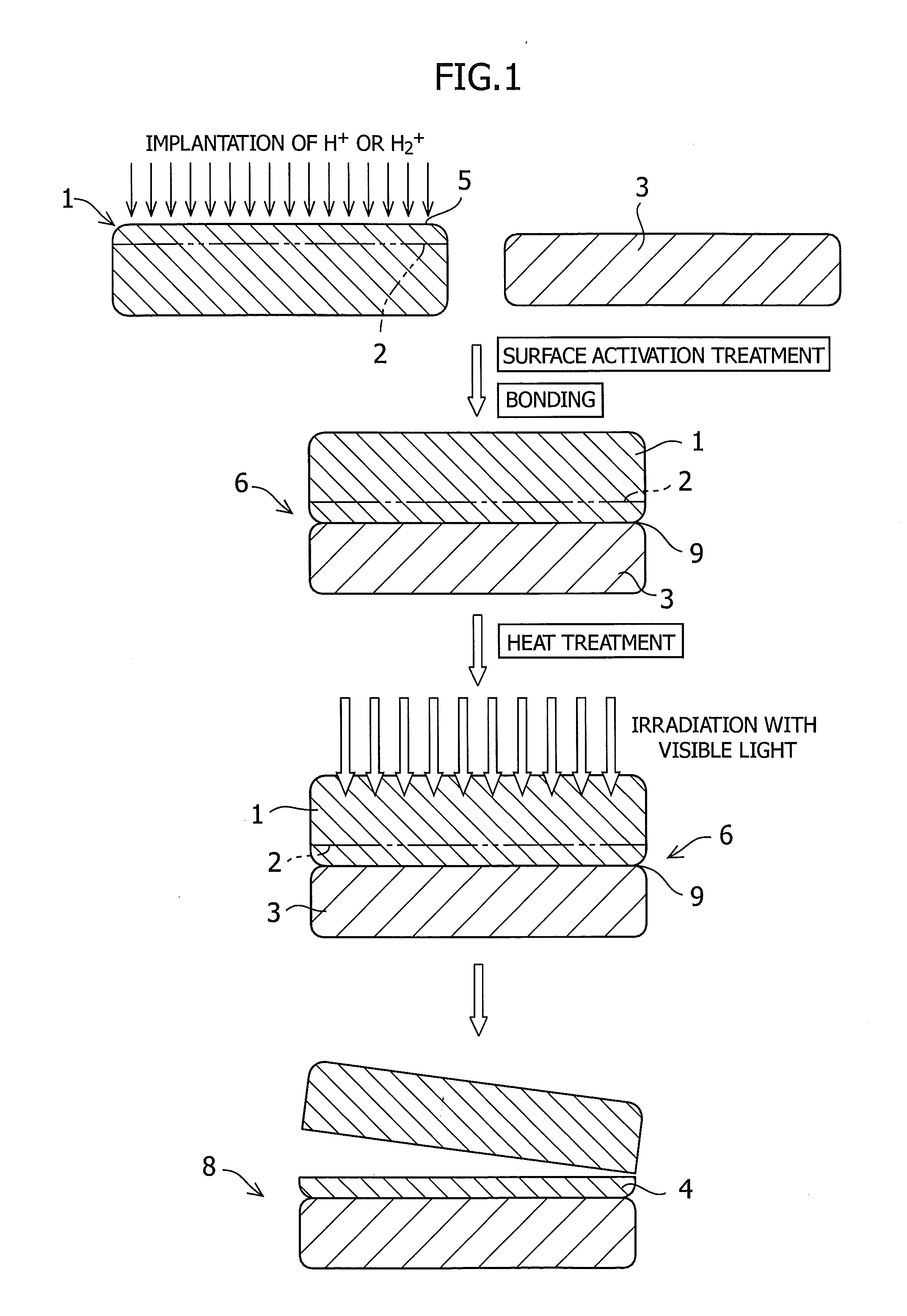
[0073]Implantation of H2+ ions into a GaN substrate of 50 mm in diameter was carried out in a dose amount of 1.35×10¹⁷ atoms / cm2 at an accelerating voltage of 75 KeV. Subsequently, a silicon substrate of 50 mm in diameter to serve as a handle substrate was prepared, and the both substrates were subjected to an ion beam activation treatment. The substrates were bonded to each other at room temperature, and subjected to a heat treatment at 250° C. for 24 hours. After preparing three sets of substrates of the same kind in total, visible light irradiation was carried out from the transparent substrate side (quartz side) with the use of a green laser (wavelength: 532 nm), RTA, or a flash lamp.

[0074]In the condition for laser irradiation in this case, the oscillation frequency was 25 mJ@3 kHz with an output of 75 W. The entire surface of the substrate was subjected to irradiation with 1.2 J / cm2.

[0075]In the case of RTA, a pyrometer was placed to observe the bonded surfaces for temperature...

example 3

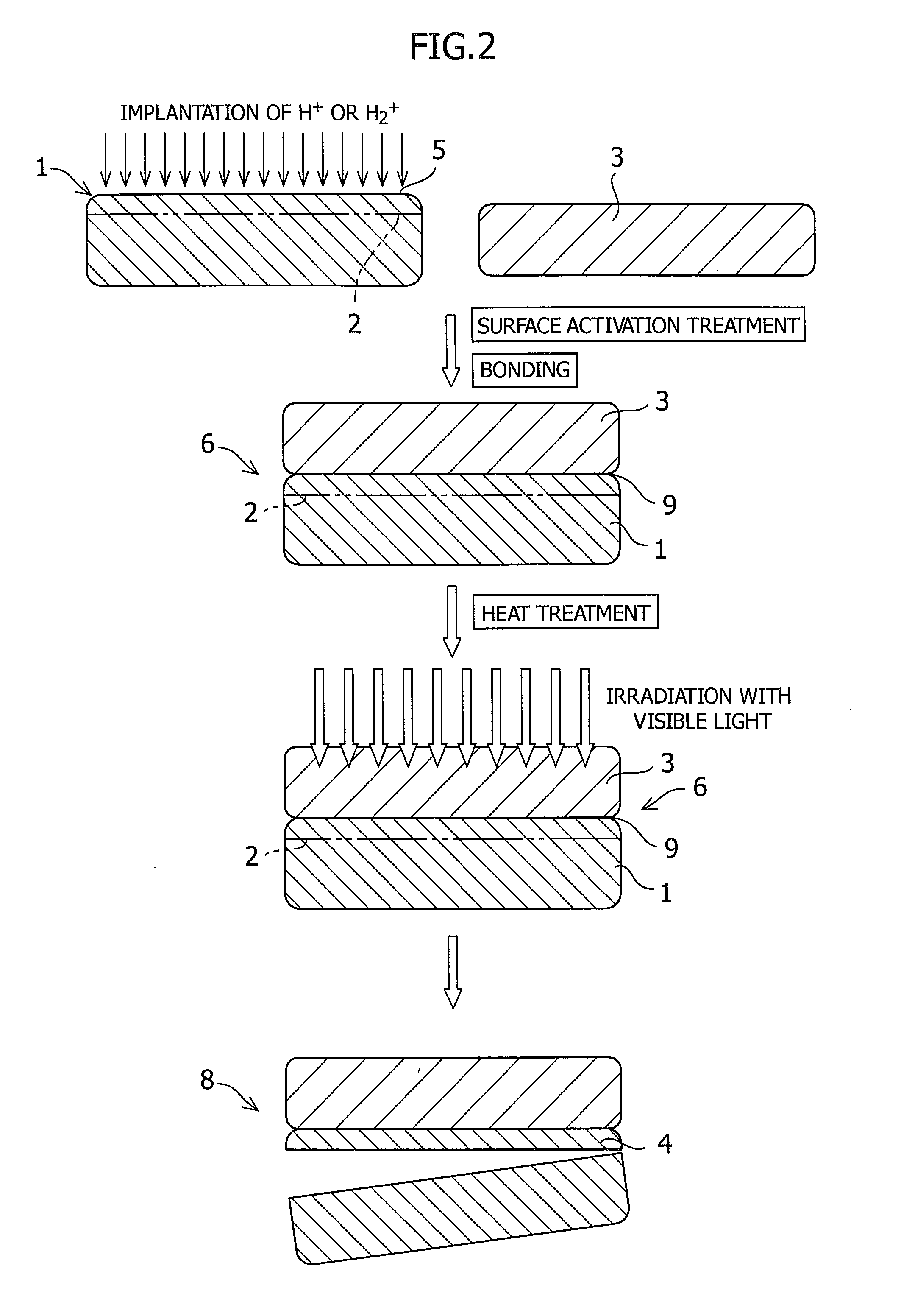
[0081]Implantation of H+ ions into a ZnO substrate of 50 mm in diameter was carried out in a dose amount of 9.5×10¹⁶ atoms / cm2 at an accelerating voltage of 80 KeV. Subsequently, a silicon substrate of 50 mm in diameter to serve as a handle substrate was prepared, and the both substrates were subjected to a plasma activation treatment. The substrates were bonded to each other at room temperature, subjected to a heat treatment at 250° C. for 24 hours, and then irradiation with a Xe flash lamp from the ZnO substrate side. The pulse width was about 1 millisecond. After the irradiation, the application of a light mechanical impact to the bonded surfaces succeeded in transfer of a film of the ZnO onto the silicon substrate. The thickness of the ZnO transferred in this case was 550 nm.


PUM


Abstract

Provided is a method for manufacturing a low-cost bonded wafer (8) which allows bulk crystals of a wide bandgap semiconductor (1) to be transferred onto a handle substrate (3) as thinly as possible without breaking the substrate. More specifically, provided is a method for manufacturing a bonded wafer (8) by forming a wide bandgap semiconductor film (4) on a surface of a handle substrate (3), the method comprising a step of implanting ions from a surface (5) of a wide bandgap semiconductor substrate (1) having a bandgap of 2.8 eV or more to form an ion-implanted layer (2), a step of applying a surface activation treatment to at least one of the surface of the handle substrate (3) and the ion-implanted surface (5) of the wide bandgap semiconductor substrate (1), a step of bonding the surface (5) of the wide bandgap semiconductor substrate (1) and the surface of the handle substrate (3) to obtain bonded substrates (6), a step of applying a heat treatment to the bonded substrates (6) at a temperature of 150° C. or more and 400° C. less, and a step of subjecting the ion-implanted layer (2) of the wide bandgap semiconductor substrate (1) to irradiation of visible light from the semiconductor substrate (1) side of the bonded substrates (6) to embrittle an interface of the ion-implanted layer (2) and transfer the wide bandgap semiconductor film (4) onto the handle substrate (3).

Description

TECHNICAL FIELD[0001]The present invention relates to a method for manufacturing a composite substrate comprising a wide bandgap semiconductor layer.BACKGROUND ART[0002]As substrates for power semiconductors and short wavelength lasers, wide bandgap semiconductors have been receiving attention in recent years. In particular, silicon carbide SiC (2.9 eV to 3.0 eV), gallium nitride GaN (3.4 eV), zinc oxide ZnO (3.37 eV), diamond (5.47 eV), aluminum nitride AN (6.0 eV) and the like, are materials particularly attracting attention, because of their high bandgaps.[0003]However, while GaN is deposited by heteroepitaxial growth on single crystalline sapphire or single crystalline SiC as an example, the deposited GaN has a lot of defects due to a difference in lattice constant, and it is now difficult to apply the GaN to power semiconductor, high-performance lasers, etc.[0004]Among methods for producing these single crystals, a method for producing the best quality crystal is a crystal grow...

Claims


Application Information

Patent Timeline
Patent Type & Authority Applications(United States)
IPC IPC(8): H01L29/161H01L21/30H01L29/20H01L29/26
CPCH01L21/76254H01L21/187H01L21/265H01L21/20
Inventor AKIYAMA, SHOJI
Owner SHIN ETSU CHEM IND CO LTD
Why Eureka
Try Eureka