Organic electroluminescence device

a technology of electroluminescence device and organic el, which is applied in the direction of thermoelectric device junction material, semiconductor device, electrical apparatus, etc., can solve the problems of reducing the yield of organic el products, the driving voltage of a phosphorescence organic el device with a high quantum efficiency of light emission, etc., and achieves high efficiency and high luminous

Inactive Publication Date: 2011-10-20
PIONEER CORP +1
View PDF4 Cites 19 Cited by
  • Summary
  • Abstract
  • Description
  • Claims
  • Application Information

AI Technical Summary

Benefits of technology

[0011]The organic electroluminescence device according to the present invention enables emission with a high luminous and high efficiency for a long life time under a low driving voltage. Therefore the organic electroluminescence device according to the present invention can adapt to a flat panel display device (e.g., a PC monitor, a wall-mounted TV), a vehicle-mounted monitor, a mobile phone display, and further to a light source with a surface emitting characteristics (e.g., a copying machine light source, a back light source of LCD or meter instruments), and it is technically valuable.

Problems solved by technology

There is a problem that a driving voltage of a phosphorescence organic EL device with a high quantum efficiency of light emission is higher than that of a fluorescence organic EL device.
In this case there is increase in occurrence of defectives electricity between both the electrodes, resulting in decrease of yields on products of the organic EL devices.

Method used


Image

  • Organic electroluminescence device
  • Organic electroluminescence device
  • Organic electroluminescence device

Examples


example 1

Performance Evaluation of Devices Using a Bulky Organic Semiconductor Compound as an Electron Injection Layer

[0072]A plurality of organic EL devices were fabricated in a manner described bellow and then the life span properties thereof were measured and evaluated.

[0073]—Elementary Device 1-1 (Ref)

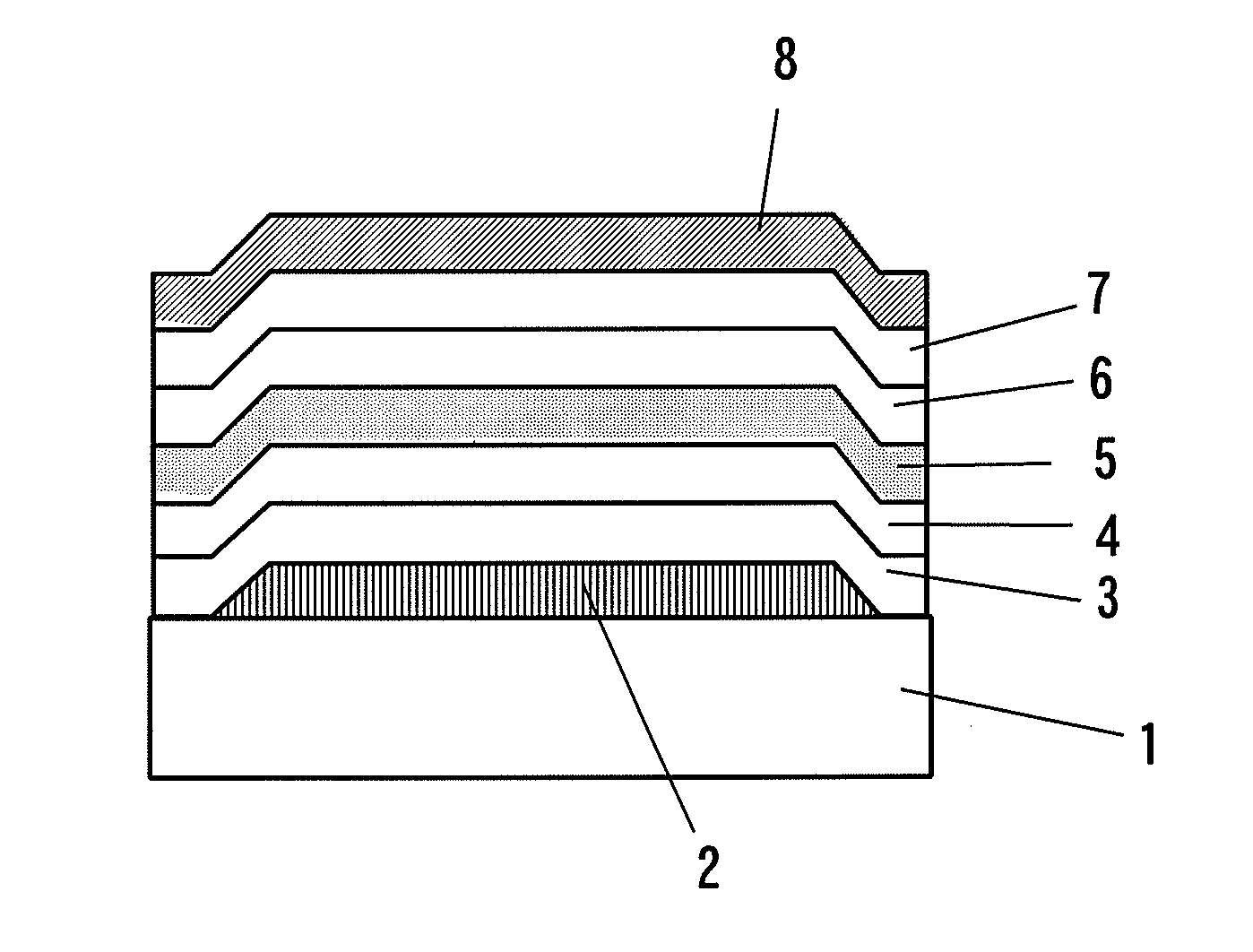
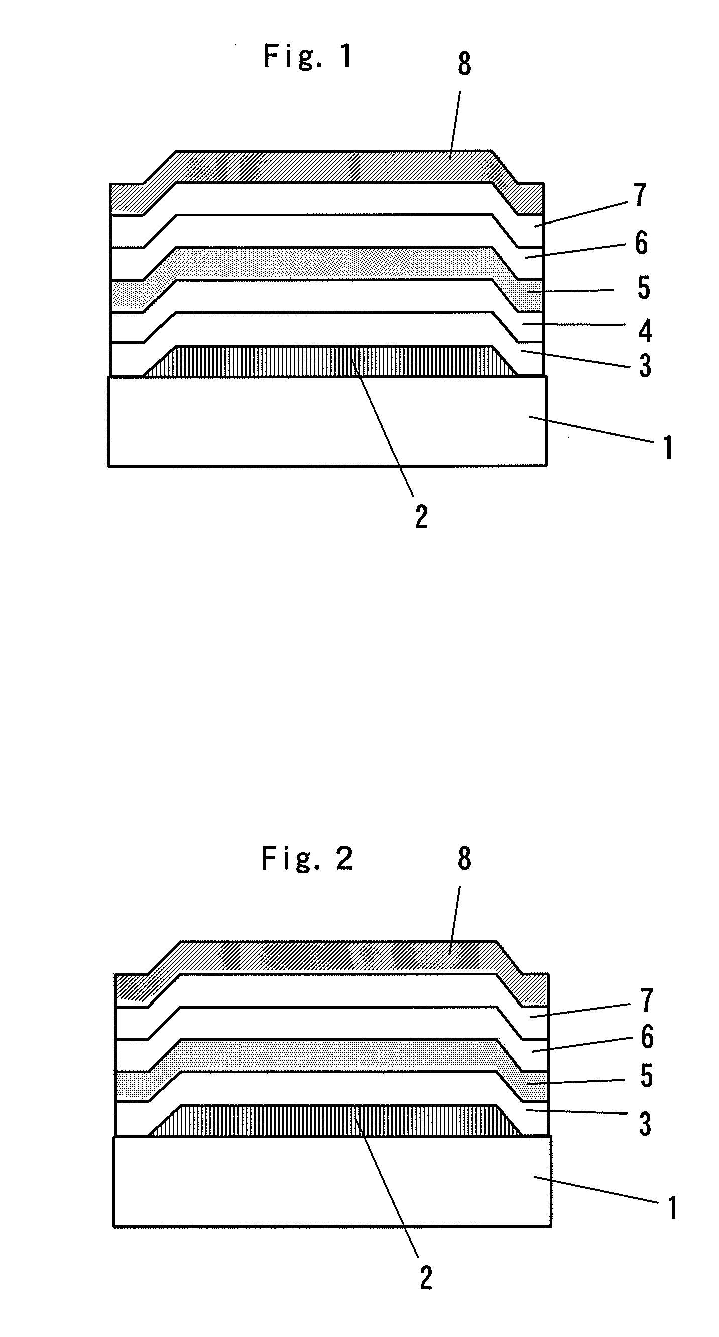
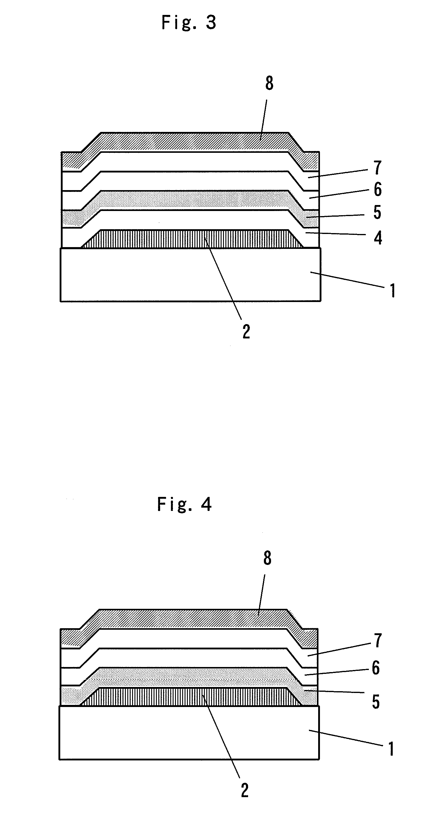
[0074]There was provided a glass substrate on which an anode of transparent electrode ITO was formed. Through a vacuum deposition method, in sequence, a hole injection layer of Copper Phthalocyanine (CuPc) with a thickness of 32 nm was formed on the anode, and then a hole transport layer of N,N′-bis(naphthalene-2-yl)-N,N′-diphenyl-benzidene (abbreviated as NPB) with a thickness of 38 nm was formed on the hole injection layer, and then a light-emitting layer functioning as an electron transport layer of Tris(8-hydroxyquinolinato)aluminum(III) (abbreviated as Alq3) with a thickness of 60 nm was formed on the hole transport layer, and then an electron injection layer Li2O (with a 10 nm thickne...

example 2

Performance Valuation of the Device Including, as a Hole Injection Layer, a Bulky Organic Semiconductor Compound Layer or an Inorganic Compound Layer Layered

[0090]A plurality of organic EL devices were fabricated in a manner described bellow and then the life span properties thereof were measured and evaluated, each of which includes a hole injection layer of inorganic compound layer (inorganic fluoride or inorganic oxide) and / or a bulky organic semiconductor compound layer (Compound 1 or Compound 4) layered.

[0091]Similarly to Example 1, the devices were based on Elementary device 1-1.

—The Device 2-2(Comparison Device 4)—

[0092]An organic EL device 2-2 was fabricated in the same manner as the Elementary device 1-1, except that a hole injection layer of MoO3 was formed with a thickness of 32 μm.

[0093]—The Device 2-3 (Corresponding to the Device 1-5: Example 1)—

[0094]An, organic EL device 2-3 was fabricated in the same manner as the Elementary device 1-1, except that a hole injection l...

example 3

Performance Valuation of the Device Including, as a Hole Injection Layer, a Mixture Layer of a Bulky Organic Semiconductor Compound and an Inorganic Compound

[0114]A plurality of organic EL devices were fabricated in a manner described bellow and then the life span properties thereof were measured and evaluated, each of which includes a hole injection layer in which an inorganic compound (inorganic fluoride, inorganic oxide) and a borazine compound (Compound 1) or benzene compound (Compound 4) are mixed.

[0115]Similarly to Example 1, the devices were based on Elementary device 1-1.

[0116]—The Device 3-2 (Corresponding to the Device 1-5: Example 1)—

[0117]An organic EL device 3-2 was fabricated in the same manner as the Elementary device 1-1, except that a hole injection layer of Compound 4 was formed with a thickness of 32 nm.

[0118]—The Device 3-3 (Corresponding to the Device 1-6: Example 2)—

[0119]An organic EL device 3-3 was fabricated in the same manner as the Elementary device 1-1, e...


PUM


Abstract

[Problem to be Solved] To provide an organic electroluminescence device with heat resistance capable of being driven by a low voltage.[Solution] An organic electroluminescence device includes a pair of anode and cathode opposed to each other; and a plurality of organic semiconductor layers layered or disposed between the anode and the cathode, the organic semiconductor layers including a light-emitting layer. At least one of the organic semiconductor layers contains a bulky organic semiconductor compound having an aromatic multi-membered ring structure and at least three aromatic substituents bonded thereto. Each of the aromatic substituents is arranged in a manner that a dihedral angle between a ring plane of the aromatic multi-membered ring structure and the ring plane of the aromatic substituent is within 70 to 90° determined by a semiempirical molecular orbital calculation method.

Description

TECHNICAL FIELD[0001]The present invention relates to organic electroluminescence devices and particularly to an organic electroluminescence (abbreviated as EL) device comprising a plurality of layered organic material layers utilizing organic compounds having electric charge-transporting properties (hole mobility and / or electron mobility).BACKGROUND ART[0002]generally, an organic EL device has a lamination structure of a plurality of layered organic material layers. The organic material layers includes an light-emitting layer and also a material layer having a hole-transporting capability such as a hole injection layer, a hole transport layer or the like, as well as another material layer having an electron transporting capability such as an electron transport layer, an electron injection layer or the like.[0003]When an electric field is applied to the multilayered organic EL films including the light-emitting layer and electron or hole transport layers etc. being layered, then hol...

Claims


Application Information

Patent Timeline
Patent Type & Authority Applications(United States)
IPC IPC(8): H01L51/54
CPCH01L51/0052H01L51/0058H01L51/5088H01L51/5048H01L51/5052H01L51/0067H10K85/626H10K85/615H10K85/654H10K50/155H10K50/165H10K50/14H10K50/17H10K50/15
Inventor OYAMADA, TAKAHITOTSUJI, TAISHIKAI, TAKAHIROOGAWA, JUNYASUDA, MITSURU
Owner PIONEER CORP
Why Eureka
Try Eureka