Single Junction CIGS/CIS Solar Module

a solar module and single junction technology, applied in the field of thin film photovoltaic modules, can solve the problems of reducing the efficiency of solar cells, so as to achieve the effect of low cost, high efficiency and simplified thin film process

Inactive Publication Date: 2011-10-27
CM MFG
View PDF5 Cites 66 Cited by
  • Summary
  • Abstract
  • Description
  • Claims
  • Application Information

AI Technical Summary

Benefits of technology

[0010]The present invention uses a process for fabricating a thin-film photovoltaic module based on a glass substrate with a form factor of 165×65 cm and larger. Advantages over conventional thin-film module includes low cost, simplified thin-film process, high efficiency with CIGS single junction photovoltaic cells with a largest monolithic panel size, and optimized pin-stripe cell pattern for maximizing photon reception. The simplified thin-film process includes preparing basic materials directly on the large sized soda lime glass substrate, including barrier material, metallic electrode material, and one or more precursor materials. Additionally, the simplified thin-film process includes a two-step process for fabricating the high efficiency copper-indium-gallium-diselenide (CIGS) photovoltaic absorber, including formin

Problems solved by technology

Unfortunately, the supply of petrochemical fuel is limited and essentially fixed based upon the amount available on the planet Earth.
Additionally, as more people use petroleum products in growing amounts, it is rapidly becoming a scarce resource, which will eventually become depleted over time.
Crystalline materials, however, are often

Method used


Image

  • Single Junction CIGS/CIS Solar Module
  • Single Junction CIGS/CIS Solar Module
  • Single Junction CIGS/CIS Solar Module

Examples


Embodiment Construction

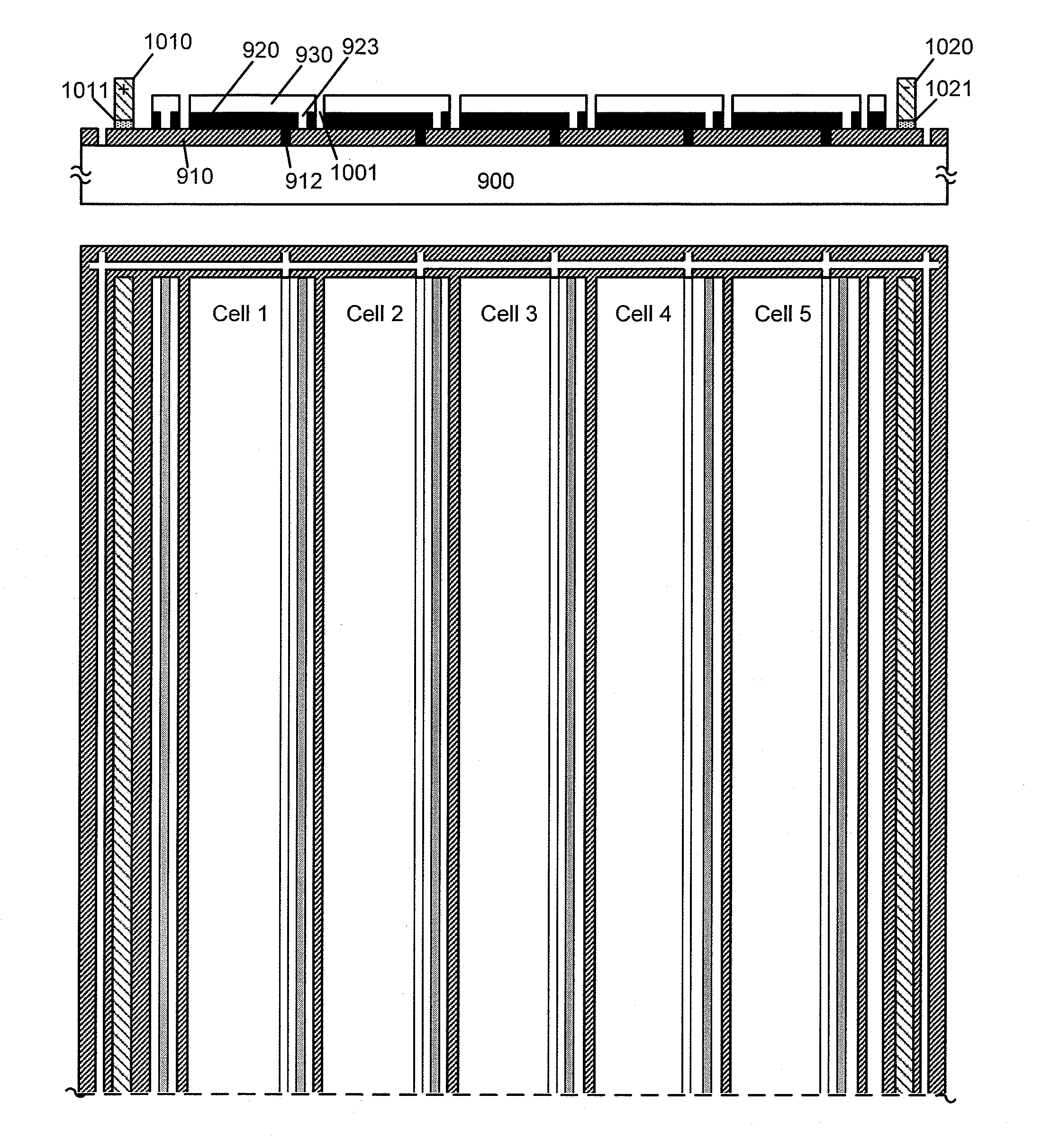
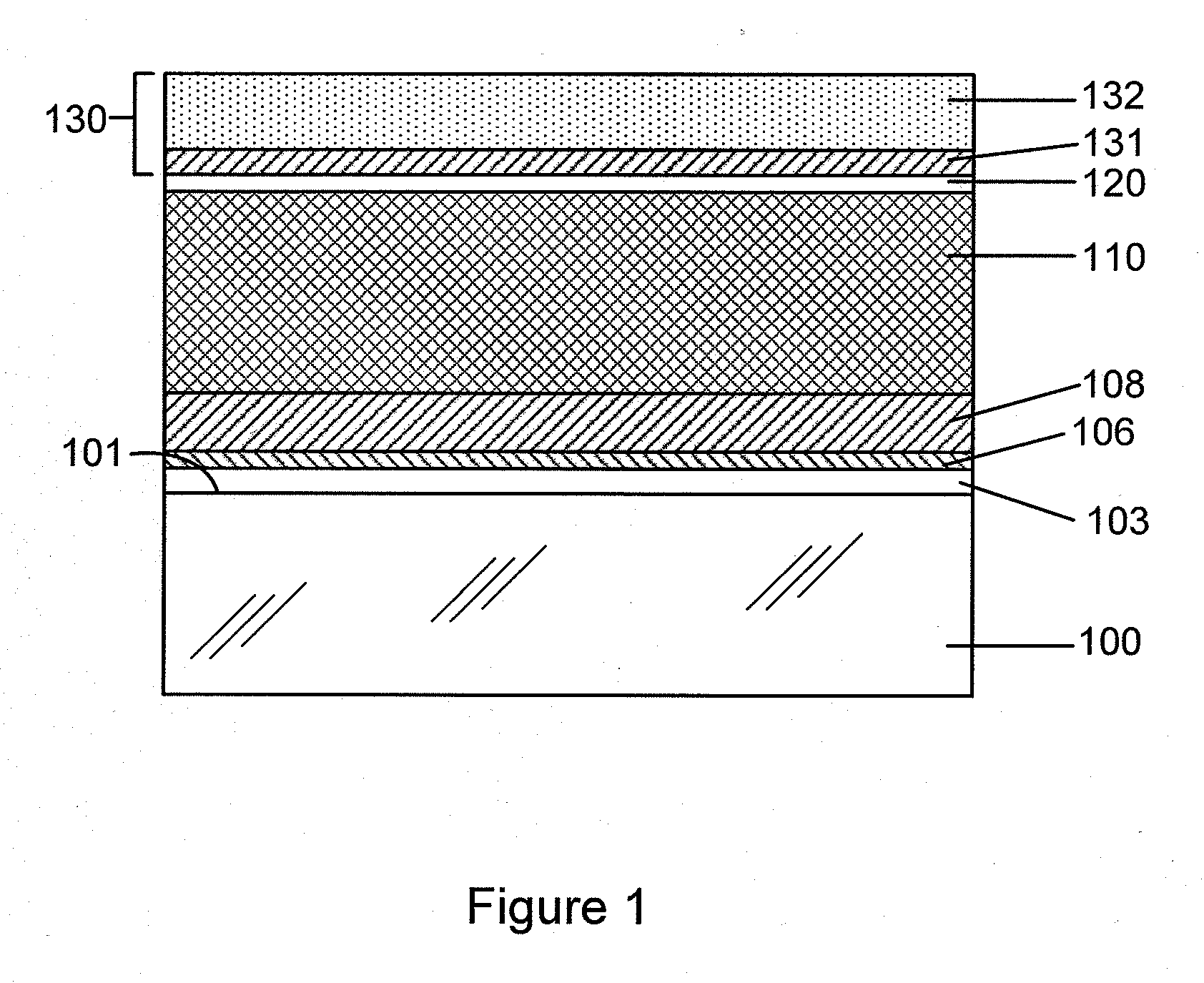
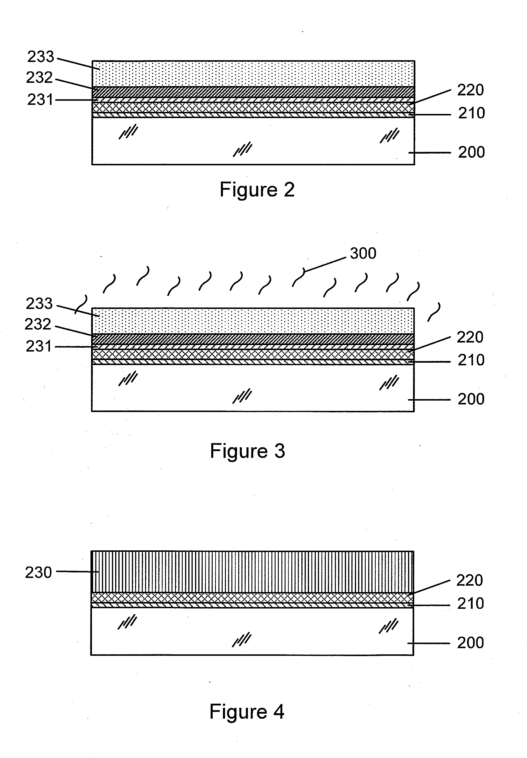
[0020]A cell structure and method for forming high efficiency thin-film photovoltaic modules are provided. The invention enables a high efficiency CIGS / CIS based thin-film photovoltaic cell from which an industrial sized panel having a form factor of 165×65 cm or greater is fabricated with a circuit efficiency of 12-15% or higher. Through work on thin-film absorber composition stoicheometry and grain structure tuning, the single junction CIGS / CIS photovoltaic absorber has an optimized opto-electric property characterized by an energy bandgap in 1.0 to 1.1 eV. This enables the cell to be used as a bottom device capable of coupling with top bi-facial devices to form a multi junction module with an enhanced module efficiency. Embodiments of the present invention may be used to include other types of semiconducting thin films or multilayers comprising iron sulfide, cadmium sulfide, zinc selenide, and others, and metal oxides such as zinc oxide, iron oxide, copper oxide, and others.

[0021...


PUM


Abstract

A high efficiency thin-film photovoltaic module is formed on a substrate. The photovoltaic module includes a plurality of stripe shaped photovoltaic cells electrically coupled to each other and physically disposed in parallel to the length one next to another across the width. Each cell includes a barrier material overlying the surface and a first electrode overlying the barrier material. Each cell further includes an absorber formed overlying the first electrode. The absorber includes a copper gallium indium diselenide compound material characterized by an energy band-gap of about 1 eV to 1.1 eV. Each cell additionally includes a buffer material overlying the absorber and a bi-layer zinc oxide material comprising a high resistivity transparent layer overlying the buffer material and a low resistivity transparent layer overlying the high resistivity transparent layer.

Description

CROSS-REFERENCE TO RELATED APPLICATION[0001]This application claims priority to U.S. Provisional Application No. 61 / 326,315, titled “HIGH EFFICIENCY CIGS / CIS SOLAR MODULE”, filed Apr. 21, 2010, by Robert D. Wieting, commonly assigned, and hereby incorporated by reference in its entirety herein for all purpose.BACKGROUND OF THE INVENTION[0002]This invention relates generally to a thin-film photovoltaic module and method of manufacturing it. More particularly, the invention provides a structure and method for manufacturing high efficiency thin film photovoltaic modules. The invention provides high efficiency thin film photovoltaic panels of a large size and with a single junction copper-indium-gallium diselenide (CIGS) cell having circuit photovoltaic efficiency of 12-15% or higher.[0003]From the beginning of time, mankind has been challenged to find way of harnessing energy. Energy comes in the forms such as petrochemical, hydroelectric, nuclear, wind, biomass, solar, and more primit...

Claims


Application Information

Patent Timeline
IPC IPC(8): H01L31/0236H01L31/18H01L27/142
CPCH01L21/02422H01L21/02488H01L21/02568Y02E10/541H01L31/022466H01L31/0322H01L31/0749H01L21/02614H01L31/022483Y02E10/547Y02P70/50
Inventor WIETING, ROBERT D.PETHE, RAJIVRAMANATHAN, KANNANSHAO, MAYTANDON, ASHISH
Owner CM MFG
Why Eureka
Try Eureka