
Power storage device and method for manufacturing the same

a technology of power storage and discharge capacity, which is applied in the manufacture of final products, electrode manufacturing processes, crystal growth processes, etc., can solve the problems of difficulty in obtaining as large a discharge capacity as the theoretical capacity, and achieve the effect of reducing increasing surface area per unit mass of the active material layer, and reducing the resistance between the current collector and the active material layer

Active Publication Date: 2011-11-03
SEMICON ENERGY LAB CO LTD
View PDF10 Cites 66 Cited by
  • Summary
  • Abstract
  • Description
  • Claims
  • Application Information

AI Technical Summary

Benefits of technology

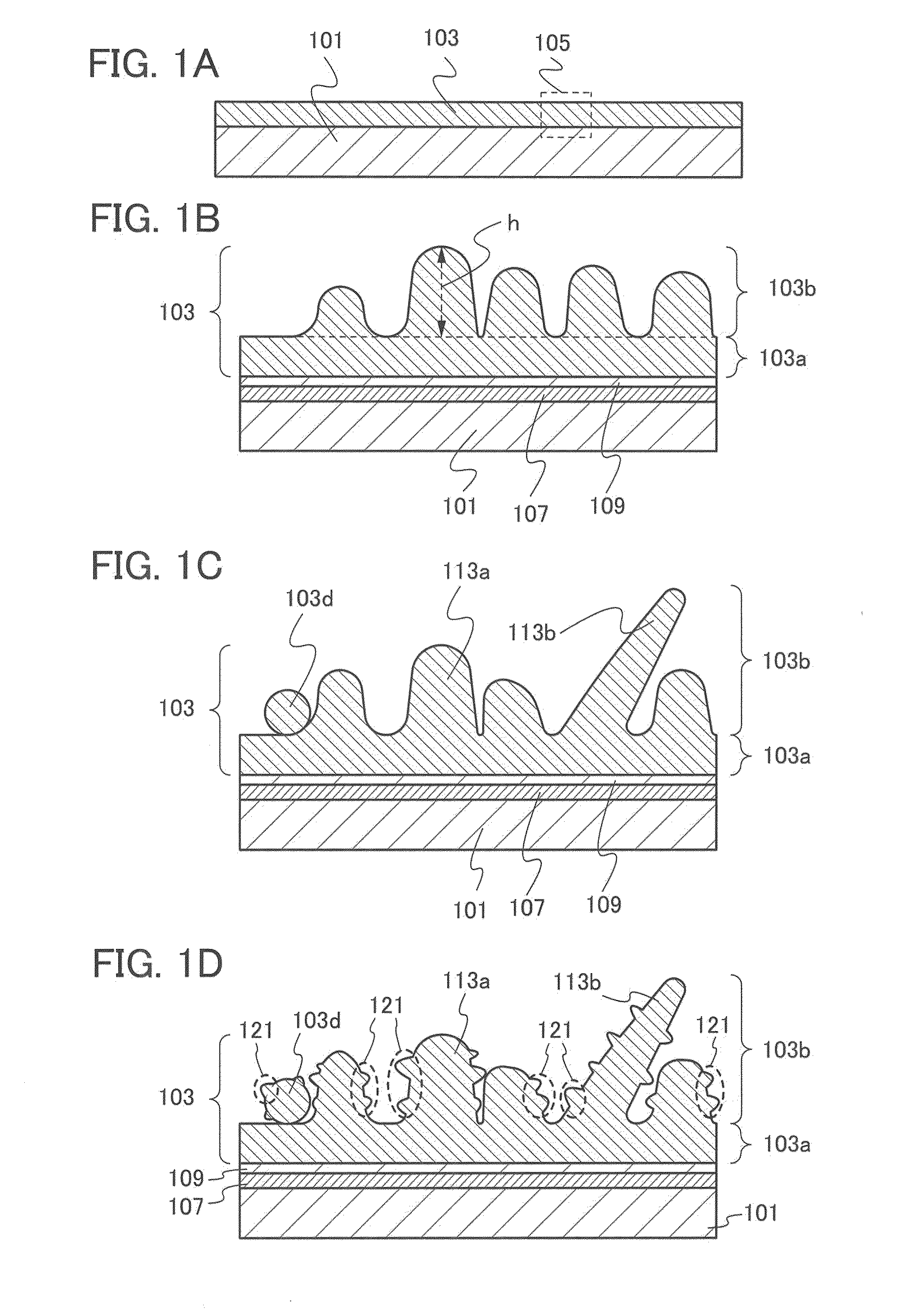
[0014]Since the crystalline silicon layer functioning as the active material layer includes the whisker-like crystalline silicon region, the surface area of the crystalline silicon layer is increased and the discharge capacity can be larger.
[0017]With the mixed layer between the current collector and the active material layer, a low-density region (a coarse region) is not formed between the current collector and the active material layer, so that interface characteristics between the current collector and the active material layer can be improved.
[0018]In addition, the metal oxide layer may be provided between the mixed layer and the active material layer. The metal oxide layer is formed using an oxide of a metal element contained in the current collector. By formation of the metal oxide layer using an oxide semiconductor, resistance between the current collector and the active material layer can be reduced, and the discharge capacity can be even larger than those of the case where the metal oxide layer is formed using an insulator.
[0019]With the above protrusions, the surface area per unit mass of the active material layer is increased. Since the surface area is increased, the rate at which a reaction substance (e.g., lithium ions) in a power storage device is adsorbed to crystalline silicon or the rate at which the reaction substance is released from the crystalline silicon becomes high per unit mass. Since the rate at which the reaction substance is adsorbed or released is high, the amount of adsorption or release of the reaction substance at a high current density is increased; therefore, the discharge capacity or charge capacity of the power storage device is larger. That is, with the use of the whisker-like crystalline silicon layer as the active material layer, the performance of the power storage device can be improved.

Problems solved by technology

However, even when silicon is used as a negative electrode active material, it is difficult to obtain as large a discharge capacity as the theoretical capacity.

Method used


Image

  • Power storage device and method for manufacturing the same
  • Power storage device and method for manufacturing the same
  • Power storage device and method for manufacturing the same

Examples


embodiment 1

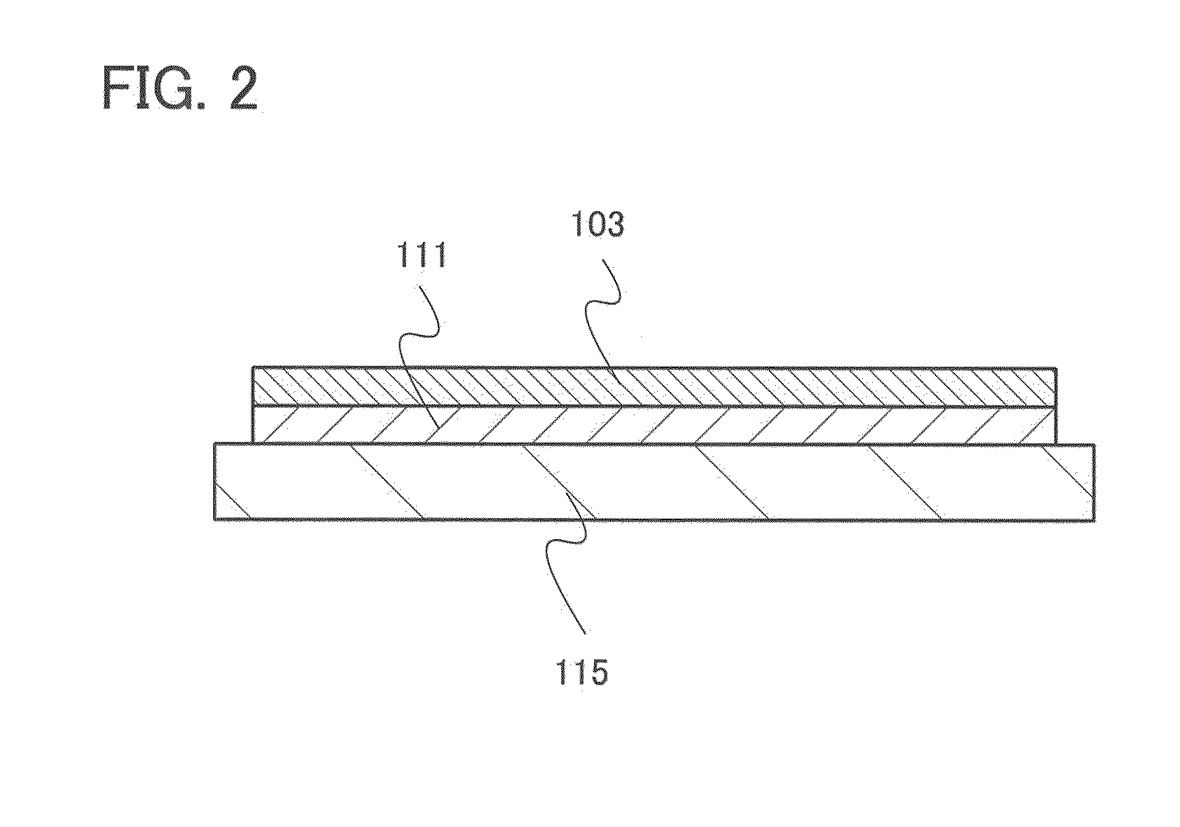
[0033]In this embodiment, an electrode for a power storage device which is one embodiment of the present invention and a method for manufacturing the electrode will be described.

[0034]The method for manufacturing the electrode of the power storage device will be described with reference to FIGS. 1A to 1D and FIG. 2.

[0035]As illustrated in FIG. 1A, a crystalline silicon layer is formed as an active material layer 103 over a current collector 101 by a thermal CVD method, preferably a low-pressure CVD method (hereinafter referred to as an LPCVD method).

[0036]The current collector 101 functions as a current collector of the electrode. Thus, a conductive material having a foil shape, a plate shape, or a net shape is used. The current collector 101 may be formed using, without a particular limitation, a metal element with high conductivity typified by platinum, aluminum, copper, or titanium. Note that the current collector 101 is preferably formed using an aluminum alloy to which an eleme...

embodiment 2

[0060]In this embodiment, a structure of a power storage device will be described with reference to FIGS. 3A and 3B.

[0061]First, a structure of a secondary battery is described below as a power storage device.

[0062]Among secondary batteries, a lithium ion battery formed using a metal oxide containing lithium, such as LiCoO2, has a large discharge capacity and high safety. Here, a structure of a lithium ion battery, which is a typical example of the secondary battery, is described.

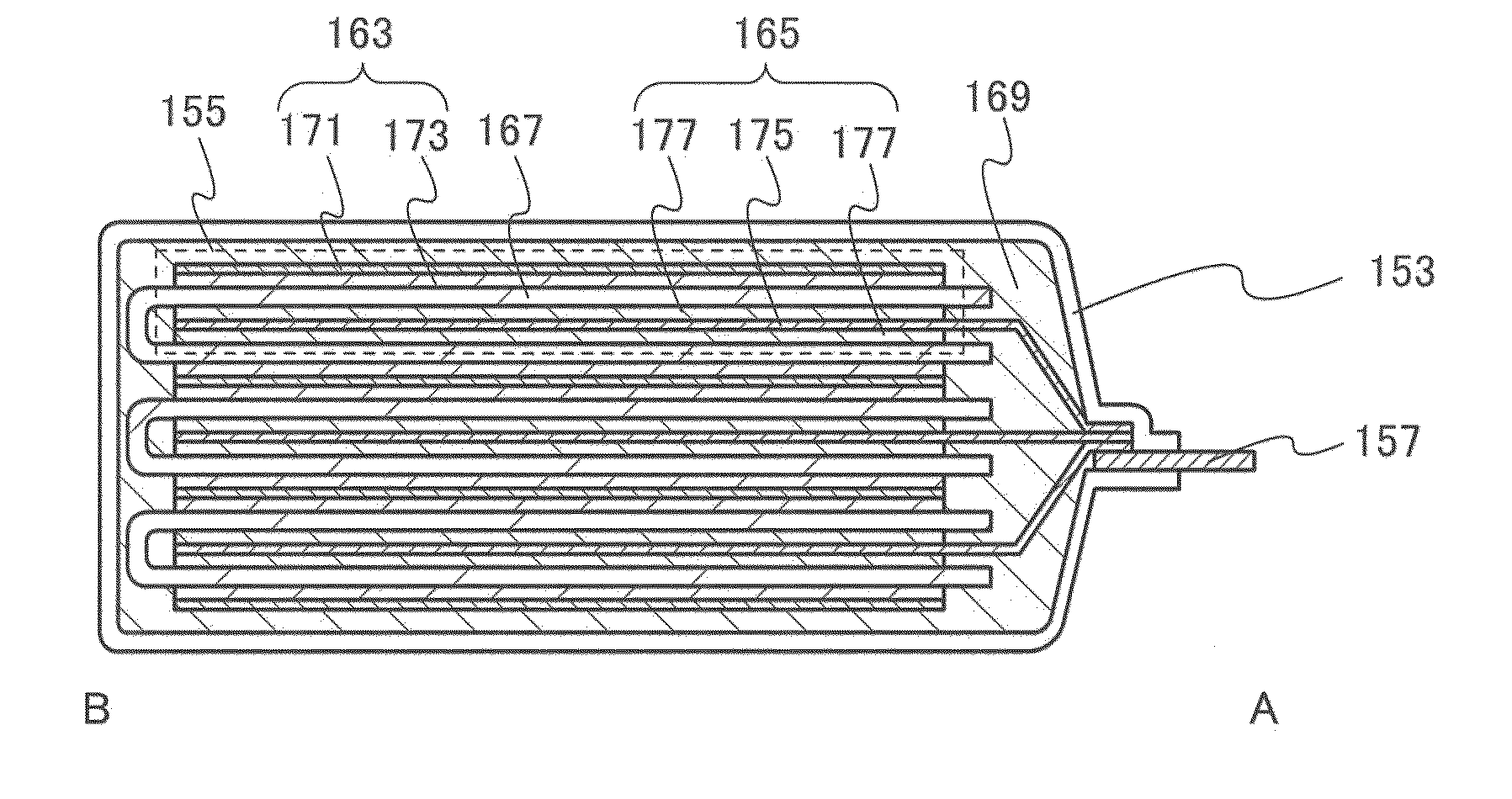
[0063]FIG. 3A is a plan-view of a power storage device 151, and FIG. 3B is a cross-sectional view taken along dot-dashed line A-B in FIG. 3A.

[0064]The power storage device 151 illustrated in FIG. 3A includes a power storage cell 155 in an exterior member 153. The power storage device 151 further includes terminal portions 157 and 159 which are connected to the power storage cell 155. For the exterior member 153, a laminate film, a polymer film, a metal film, a metal case, a plastic case, or the like can be ...

embodiment 3

[0084]In this embodiment, an application example of the power storage device described in Embodiment 2 is described with reference to FIGS. 4A and 4B.

[0085]The power storage device described in Embodiment 2 can be used in electronic devices, e.g., cameras such as digital cameras or video cameras, digital photo frames, mobile phones (also referred to as cellular phones or cellular phone devices), portable game machines, portable information terminals, or audio reproducing devices. Further, the power storage device can be used in electric propulsion vehicles such as electric vehicles, hybrid electric vehicles, train vehicles, maintenance vehicles, carts, or wheelchairs. Here, as a typical example of the electric propulsion vehicles, a wheelchair is described.

[0086]FIG. 4A is a perspective view of an electric wheelchair 501. The electric wheelchair 501 includes a seat 503 where a user sits down, a backrest 505 provided behind the seat 503, a footrest 507 provided at the front of and be...


PUM

PropertyMeasurementUnit
temperatureaaaaaaaaaa
widthaaaaaaaaaa
widthaaaaaaaaaa

Abstract

Provided is a method for manufacturing a power storage device in which a crystalline silicon layer including a whisker-like crystalline silicon region is formed as an active material layer over a current collector by a low-pressure CVD method in which heating is performed using a deposition gas containing silicon. The power storage device includes the current collector, a mixed layer formed over the current collector, and the crystalline silicon layer functioning as the active material layer formed over the mixed layer. The crystalline silicon layer includes a crystalline silicon region and a whisker-like crystalline silicon region including a plurality of protrusions which project over the crystalline silicon region. With the protrusions, the surface area of the crystalline silicon layer functioning as the active material layer can be increased.

Description

TECHNICAL FIELD[0001]The present invention relates to a power storage device and a method for manufacturing the power storage device.[0002]Note that the power storage device indicates all elements and devices which have a function of storing power.BACKGROUND ART[0003]In recent years, power storage devices such as lithium-ion secondary batteries, lithium-ion capacitors, and air cells have been developed.[0004]An electrode for the power storage device is manufactured by providing an active material over a surface of a current collector. As the active material, a material which can adsorb and release ions functioning as carriers, such as carbon or silicon, is used. For example, silicon or phosphorus-doped silicon has an advantage of larger theoretical capacity than carbon and larger capacity of a power storage device (e.g., Patent Document 1).REFERENCEPatent Document[0005][Patent Document I] Japanese Published Patent Application No. 2001-210315DISCLOSURE OF INVENTION[0006]However, even...

Claims


Application Information

Patent Timeline
Patent Type & Authority Applications(United States)
IPC IPC(8): H01L29/02H01L21/02H01G9/00H01G11/06H01G11/22H01G11/24H01G11/26H01G11/30H01G11/46H01G11/66H01G11/68H01G11/70H01G11/84H01G11/86H01M4/134H01M4/1395H01M4/38H01M4/64H01M4/66
CPCH01G11/06Y02T10/7011H01G11/30H01G11/46H01G11/50H01L21/02532H01L21/02587H01L21/0262H01L28/82Y02T10/7022H01G11/26Y02E60/13Y02E60/122H01M4/0428H01M4/134H01M4/1395H01M4/386H01M4/661H01M4/667H01M10/0525H01M10/0583C30B25/005C30B29/06C30B29/62C30B33/02H01G11/28Y02E60/10Y02T10/70Y02P70/50H01G11/22H01G11/68H01G11/70H01M4/382H01M10/0569H01M12/08H01M2300/0037
Inventor KURIKI, KAZUTAKAYUKAWA, MIKIOASANO, YUJI
Owner SEMICON ENERGY LAB CO LTD
Learn More