Diamond neural devices and associated methods

a neural device and diamond technology, applied in the field of diamond neural devices, can solve the problems of increasing the complexity of substrate preparation and growth procedures, coatings can also be undesirable for in vivo use, and protein coatings

Inactive Publication Date: 2011-11-17
SUNG CHIEN MIN
View PDF2 Cites 24 Cited by
  • Summary
  • Abstract
  • Description
  • Claims
  • Application Information

AI Technical Summary

Problems solved by technology

Protein coatings can increase the complexity of the substrate preparation and growth procedures.
Such coatings can also be undesirable for in vivo use.

Method used


Image

  • Diamond neural devices and associated methods
  • Diamond neural devices and associated methods
  • Diamond neural devices and associated methods

Examples


example 1

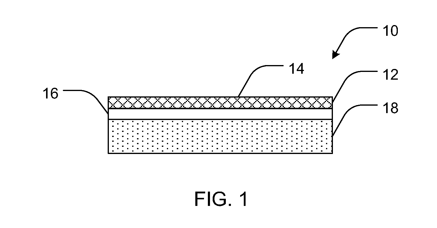
[0068]A silicon wafer is seeded with nanodiamond in an ultrasonic bath. The nanodiamond seeded wafer is grown in a microwave plasma CVD reactor that is purged with methane / trimethyl boride, and an abundance of hydrogen. As a result, a layer of boron doped diamond (BDD) is grown on nanodiamond seeds to a thickness of about 10 microns. The BDD is electrically conducting but with a semiconductor bandgap. BDD is subsequently graded to BN / AN / GaN / InN by Atomic Layer Deposition (ALD). This graded material can absorb across the entire spectrum of visible light and some UV. The Si wafer is etched away with concentrated KOH solution to expose the BDD with the surface protruded with high density nuclei (about one trillion per square centimeter) of nanodiamond.

example 2

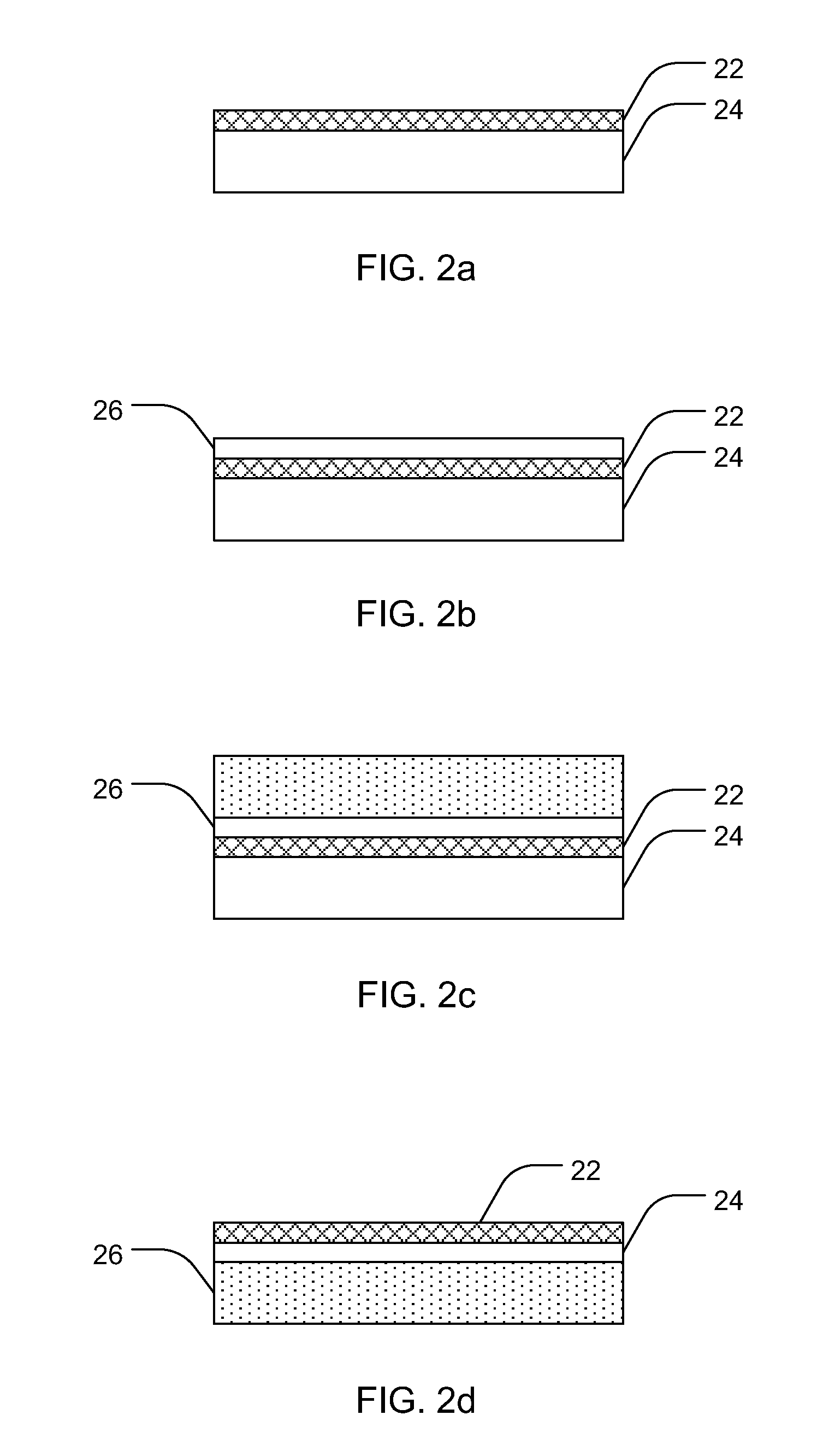
[0069]In this example, nitride semiconductors are not used. BDD is back converted to make graphene on the surface. A (100) face can form graphene perpendicular to the surface. Such perpendicular oriented graphene can act as an emitting antenna because graphene has minimal electrical resistance. Graphene can transmit terahertz signals due to its high stiffness. On the other hand, a (111) face can form graphene layers in parallel to the surface by straightening the puckered hexagons of carbon atoms. Such a parallel orientation can be used as a receiver for signals. Graphene is also a piezoelectric layer on diamond surface so radiation signals can be converted to phonons (lattice vibrations) vice versa.

example 3

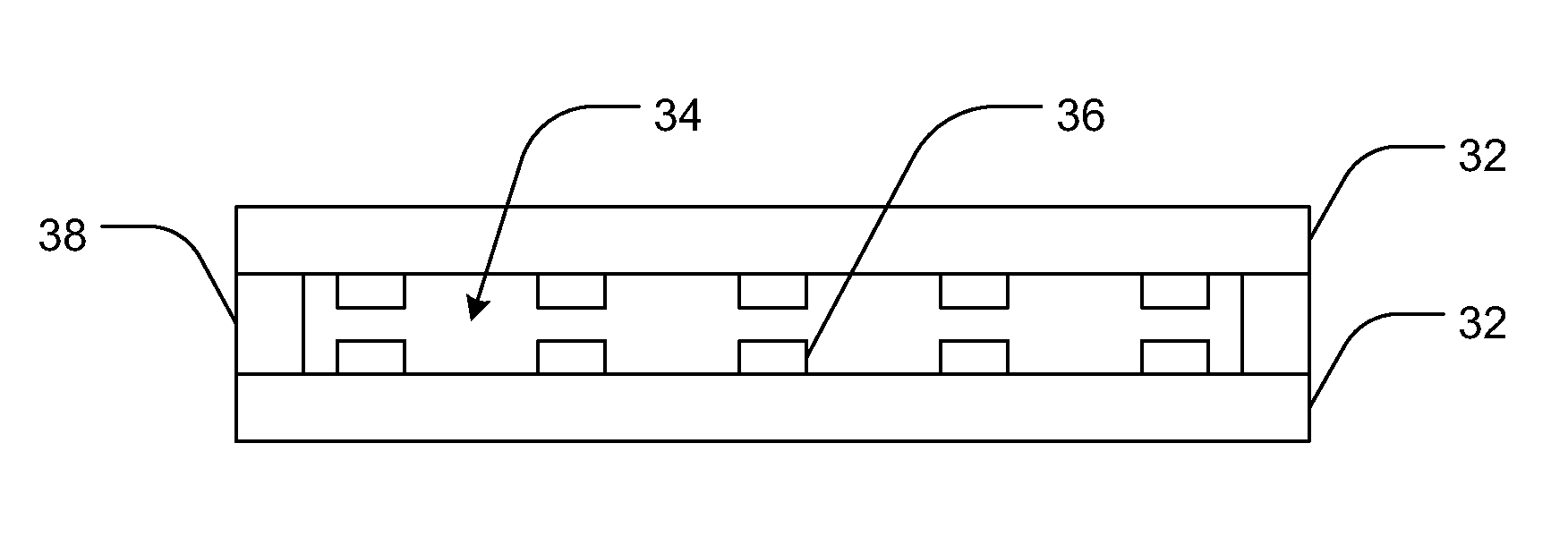
[0070]A small single crystal diamond made (twins with triangular shape, typically flat) is etched in oxygen plasma to form a frosted surface with nano-sized protrusions. A boron-doped diamond layer is CVD deposited on the other side of the made from the frosted surface using BCl3 and CH4 diluted in H2. The CH4 is replaced with NH3 to grow a layer of cubic BN (cBN). The cBN is doped with C or Si by ion implantation followed by annealing. The result is a p-type boron-doped diamond and n-type cBN structure with nanodiamond protrusion on one side that can be used to anchor neurons.


PUM

PropertyMeasurementUnit
bond lengthaaaaaaaaaa
thickaaaaaaaaaa
thickaaaaaaaaaa

Abstract

The present disclosure provides devices for neuronal growth and associate methods. In one aspect, for example, a neuronal growth device is provided including a layer of nanodiamond particles having an exposed neuronal growth surface, a doped diamond layer contacting the layer of nanodiamond particles opposite the neuronal growth surface, and a semiconductor layer coupled to the doped diamond layer opposite the layer of nanodiamond particles. In one aspect, the nanodiamond particles are substantially immobilized by the doped diamond layer.

Description

PRIORITY DATA[0001]This application claims the benefit of U.S. Provisional Patent Application Ser. No. 61 / 333,629, filed on May 11, 2010, which is incorporated herein by reference in its entirety.BACKGROUND OF THE INVENTION[0002]Growth surfaces for neurons and other cellular material has proven challenging. In adhesion of neurons, for example, too many substrates are problematic, requiring complex protein coatings to be applied to the substrates. Such protein coatings are difficult to apply and may be less desirable for use in chronic neural implants. These protein materials may be toxic at some level, and in some cases may alter the normal growth and function of surrounding neurons.[0003]Additionally, various groups have attempted to interface neuronal material with electronic devices with little success. Materials that can provide adequate anchoring of neurons are generally not conducive to integration with electronic devices. Similarly, materials that incorporate well into electr...

Claims


Application Information

Patent Timeline
Patent Type & Authority Applications(United States)
IPC IPC(8): A61N1/05B82Y5/00B82Y40/00H01L21/04
CPCC12N2533/10C12N5/0619
Inventor SUNG, CHIEN-MIN
Owner SUNG CHIEN MIN
Why Eureka
Try Eureka