Pillar structure for memory device and method

a memory device and pillar structure technology, applied in the field of switching devices, can solve the problems of dielectric breakdown, reduced device size, and inability to operate properly, and achieve the effect of a wide range of application and high density memory

Active Publication Date: 2011-12-22
CROSSBAR INC
View PDF3 Cites 77 Cited by
  • Summary
  • Abstract
  • Description
  • Claims
  • Application Information

AI Technical Summary

Benefits of technology

[0005]The present invention is directed to memory devices. More particularly, embodiments according to the present invention provide a method to form a plurality of pillar structures for an array of switching devices. The pillar struct

Problems solved by technology

However, as field effect transistor (FET) approach sizes less than 100 nm, problems such as short channel effect start to prevent proper device operation.
Moreover, transistor based memories such as those commonly known as Flash can have additional performance degradations as device sizes shrink.
The high voltage can result in dielectric breakdown and increases the possibility of disturb mechanisms.
However, these new memory cells usually lack one or more key attributes, which have prevented their widespread adoption in high vo

Method used


Image

  • Pillar structure for memory device and method
  • Pillar structure for memory device and method
  • Pillar structure for memory device and method

Examples


Embodiment Construction

[0010]The present invention is generally related to a switching device. More particularly, embodiments of the present invention provide a structure and a method for forming a plurality of resistive switching devices each having a pillar structure. The present invention has been applied to fabrication of high density non-volatile memory devices. But it should be recognize that embodiments according to the present invention would have a much broader range of applicability.

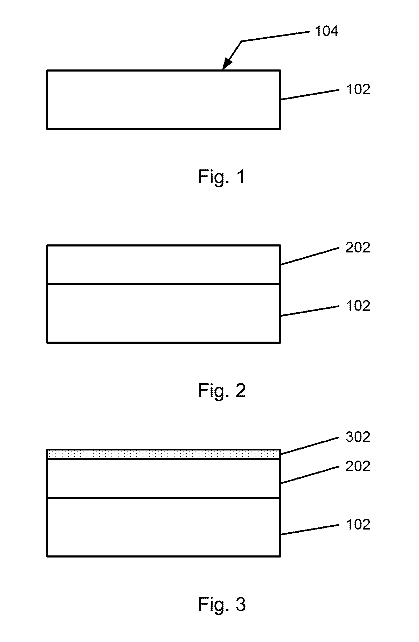
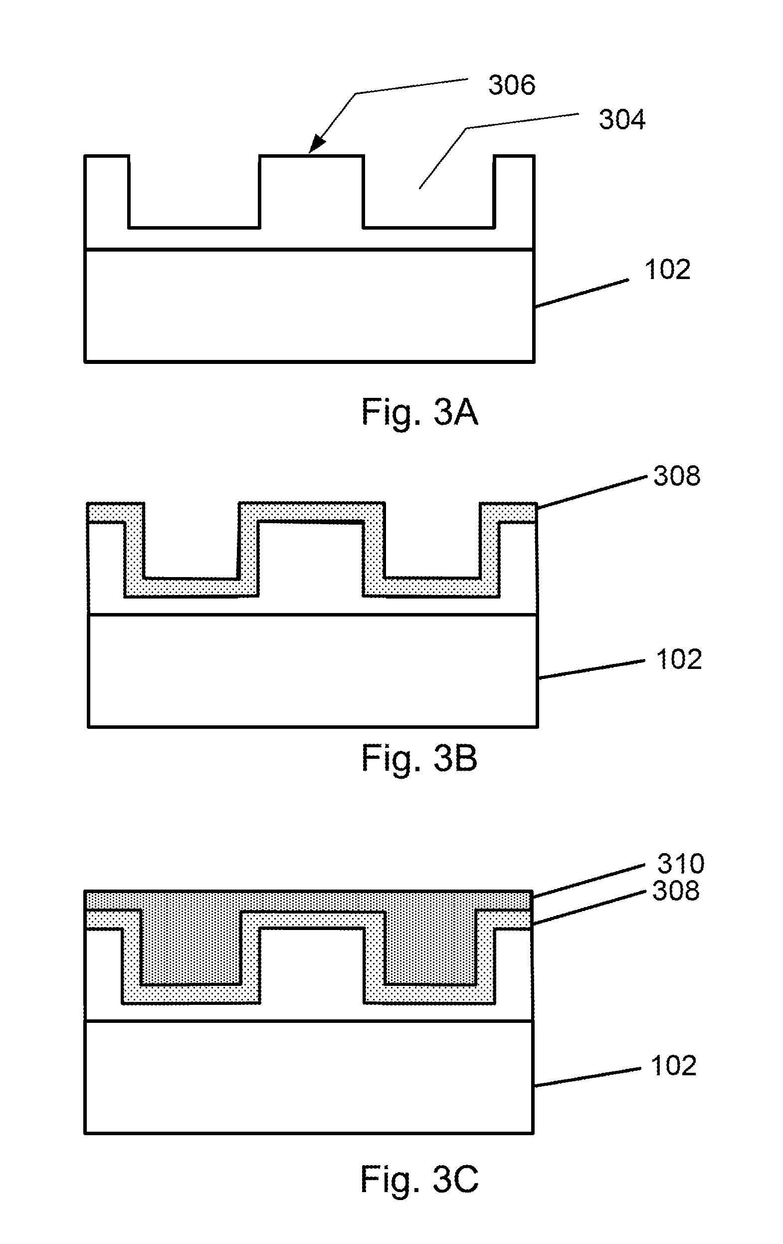
[0011]FIGS. 1-17 illustrate a method of forming a switching device according to embodiments of the present invention. These diagrams are merely examples and should not unduly limit the claims herein. One skilled in the art would recognize other variations, modifications, and alternatives.

[0012]As shown in FIG. 1, a substrate 102 having a surface region 104 is provided. The substrate can be a semiconductor substrate in a specific embodiment. The semiconductor substrate can be a single crystal silicon wafer, a silicon ...


PUM


Abstract

A method of forming a memory device. The method provides a semiconductor substrate having a surface region. A first dielectric layer is formed overlying the surface region of the semiconductor substrate. A bottom wiring structure is formed overlying the first dielectric layer and a second dielectric material is formed overlying the top wiring structure. A bottom metal barrier material is formed to provide a metal-to-metal contact with the bottom wiring structure. The method forms a pillar structure by patterning and etching a material stack including the bottom metal barrier material, a contact material, a switching material, a conductive material, and a top barrier material. The pillar structure maintains a metal-to-metal contact with the bottom wiring structure regardless of the alignment of the pillar structure with the bottom wiring structure during etching. A top wiring structure is formed overlying the pillar structure at an angle to the bottom wiring structure.

Description

BACKGROUND[0001]The present invention is related to switching devices. More particularly, the present invention provides a structure and a method for forming a non-volatile resistive switching memory device having desirable characteristics.[0002]The success of semiconductor devices has been mainly driven by an intensive transistor down-scaling process. However, as field effect transistor (FET) approach sizes less than 100 nm, problems such as short channel effect start to prevent proper device operation. Moreover, transistor based memories such as those commonly known as Flash can have additional performance degradations as device sizes shrink. For example, a high voltage is usually required for programming of a Flash memory device. The high voltage can result in dielectric breakdown and increases the possibility of disturb mechanisms. Flash memory is one type of non-volatile memory device.[0003]Other non-volatile random access memory (RAM) devices such as ferroelectric RAM (Fe RAM)...

Claims


Application Information

Patent Timeline
IPC IPC(8): H01L21/205
CPCH01L45/148H01L45/1675H01L45/1666H01L45/1608H10B63/80H10N70/245H10N70/884H10N70/826H10N70/023H10N70/063H10N70/20H10N70/021H10N70/061
Inventor HERNER, SCOTT BRAD
Owner CROSSBAR INC
Why Eureka
Try Eureka