Flexible ferroelectric memory device and manufacturing method for the same

a ferroelectric memory and non-volatile technology, applied in the direction of digital storage, semiconductor devices, instruments, etc., can solve the problems of difficult to form a stable interface between a ferroelectric material and a semiconductor material, the type of materials suitable for this process is limited, and the performance of as-fabricated devices is relatively low. , to achieve the effect of excellent electrical and mechanical properties and ease of processing

Inactive Publication Date: 2011-12-29
RES & BUSINESS FOUND SUNGKYUNKWAN UNIV
View PDF2 Cites 23 Cited by
  • Summary
  • Abstract
  • Description
  • Claims
  • Application Information

AI Technical Summary

Benefits of technology

[0043]In accordance with the present disclosure, a transistor-type flexible nonvolatile ferroelectric memory device showing excellent electrical and mechanical properties and having flexibility, a 1T-1R flexible ferroelectric memory device, and a manufacturing method for the same are provided, and these technologies can be applied to a flexible electric and electronic system in various ways. Further, in accordance with the present disclosure, a ferroelectric layer is formed and transferred onto a flexible substrate so as to manufacture a transistor-type flexible nonvolatile ferroelectric memory device, and, thus, the memory device may have a wide range of applications owing to easiness in processing and suitability in continuous processes.

Problems solved by technology

A capacitor-type device is a nonvolatile device but destroys data while reading the data, and, thus, the capacitor-type device needs to store the data again after reading the data.
Meanwhile, it is difficult to form a stable interface between a ferroelectric material and a semiconductor material, and, thus, a further study on a structure employing a dielectric film (MFIS structure) or a metal film and a dielectric film (MFMIS) serving as a buffer layer between the ferroelectric material and the semiconductor material is needed.
However, a low degree of crystallinity associated with classes of materials results in relatively low performance of the as-fabricated devices.
However, types of materials suitable for this process are limited.

Method used


Image

  • Flexible ferroelectric memory device and manufacturing method for the same
  • Flexible ferroelectric memory device and manufacturing method for the same
  • Flexible ferroelectric memory device and manufacturing method for the same

Examples


example 1

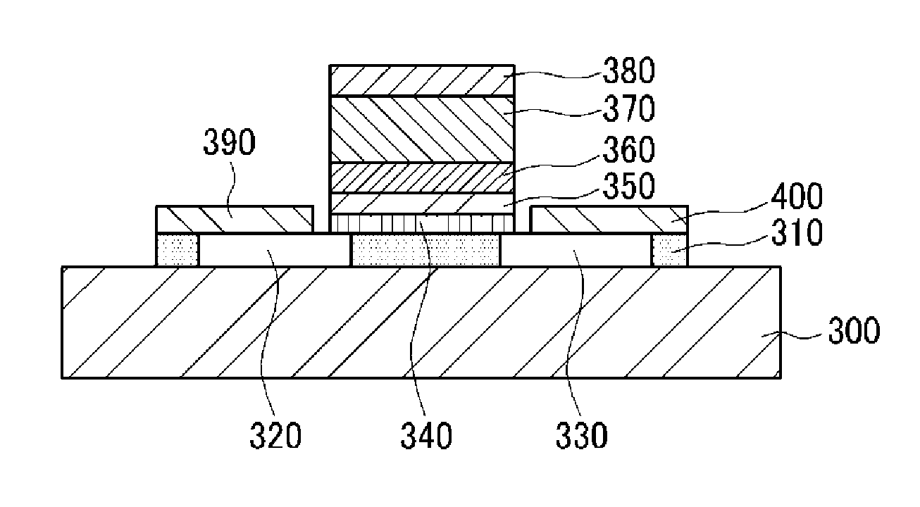
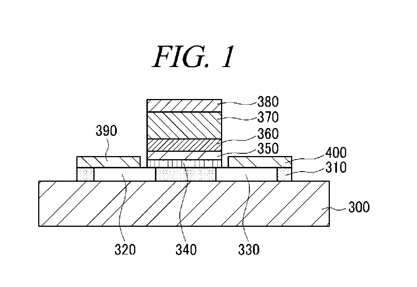
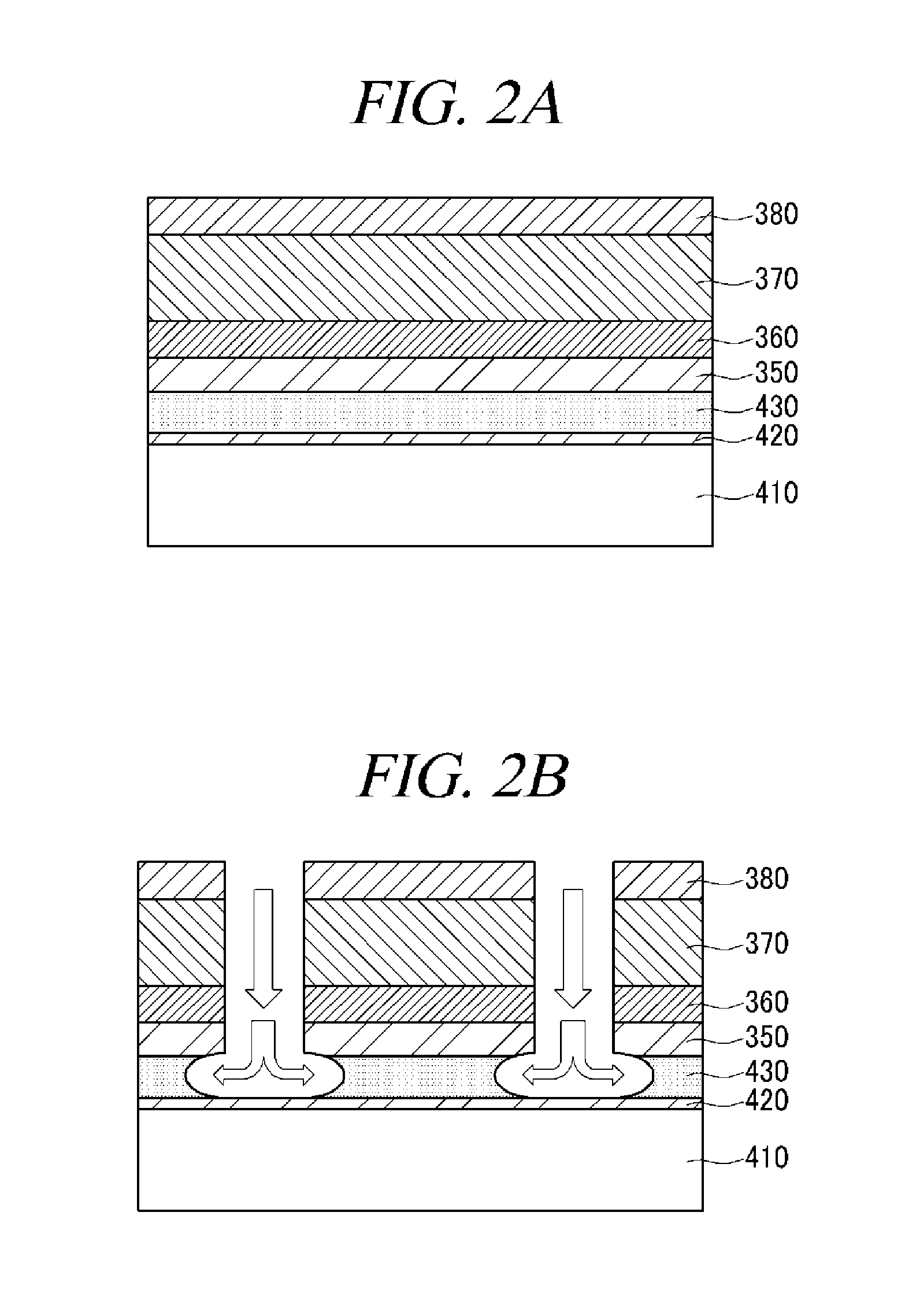
[0099]Ferroelectric Thin Film Transistor for Flexible Ferroelectric Memory Device

[0100]A lower electrode was formed by depositing Pt (about 80 nm) and Ti (about 20 nm) on a SiO2 (about 300 nm) / Si substrate by using a RF sputter. A ferroelectric material, PZT was formed to have a thickness of about 360 nm by a sol-gel method and then was preformed a heat treatment at about 650° C. for about 30 minutes to impart high polarization property. After source / drain regions were heavily n-doped on a lightly p-doped SOI substrate and a sacrificial layer was removed with hydrofluoric acid, a silicon thin film to be transferred onto the PZT substrate PZT was separated from a mother substrate by using a rubber stamp. A PZT / Pt / Ti / SiO2 / Si substrate was spin-coated with 10%-diluted Su-8 and treated UV for about 10 seconds, and the rubber stamp with a Si thin film attached thereto was brought into contact with the Su-8. While the Su-8 and the Si thin film were in contact with each other, they were un...


PUM


Abstract

The present disclosure relates to a flexible nonvolatile ferroelectric memory device, a 1T-1R (1Transistor-1Resistor) flexible ferroelectric memory device, and a manufacturing method for the same.

Description

CROSS-REFERENCE TO RELATED APPLICATION[0001]This application claims the benefit of Korean Patent Application 10-2010-0062280, filed on Jun. 29, 2010, which is incorporated herein by reference.FIELD OF THE INVENTION[0002]The present disclosure relates to a flexible nonvolatile ferroelectric memory device, a 1T-1R (1Transistor-1Resistor) flexible ferroelectric memory device, and a manufacturing method for the same.BACKGROUND OF THE INVENTION[0003]A FeRAM (or FRAM) using a ferroelectric material having spontaneous polarization is a memory that stores “1” and “0” bits using remanent polarization and has attracted attention as a next-generation memory device since it has a lot of advantages such as low power consumption, rapid processing speed, and a simple configuration. The FeRAM stores information in two different types: a capacitor type (1 Transistor-1 capacitor type) in which a dielectric material of a capacitor of a DRAM is simply substituted by a ferroelectric material; and a tran...

Claims


Application Information

Patent Timeline
Patent Type & Authority Applications(United States)
IPC IPC(8): H01L29/78H01L21/336
CPCH01L21/28291H01L21/84H01L27/1159H01L29/78391H01L28/24H01L29/6684G11C11/22H01L27/1203H01L29/40111H10B51/30
Inventor AHN, JONG-HYUNRHO, JONGHYUN
Owner RES & BUSINESS FOUND SUNGKYUNKWAN UNIV
Why Eureka
Try Eureka