Temporary bonding adhesive for a semiconductor wafer and method for manufacturing a semiconductor device using the same

a technology of semiconductor wafers and adhesives, which is applied in the direction of solid-state devices, polyamide coatings, coatings, etc., can solve the problems of increased adhesion of bg tapes, increased thickness of ground wafers, and increased thickness of required thicknesses. , to achieve the effect of reducing the damage of semiconductor wafers, high precision processing, and easy detachment of semiconductor wafers after processing

Active Publication Date: 2011-12-29
SUMITOMO BAKELITE CO LTD
View PDF6 Cites 80 Cited by
  • Summary
  • Abstract
  • Description
  • Claims
  • Application Information

AI Technical Summary

Benefits of technology

[0015]The aim of the present invention is to provide a temporary bonding adhesive for a semiconductor wafer that reduces damage to the semiconductor wafer, allows for high precision processing, and for which the detachment of the semiconductor wafer after processing is easy, and a method for manufacturing a semiconductor device that reduces damage to the semiconductor wafer, allows for high precision processing, and can shorten the time needed for thermal decomposition.
[0016]According to the present invention, a temporary bonding adhesive for a semiconductor wafer is provided that temporarily bonds a semiconductor wafer to a supporting substrate for processing the semiconductor wafer, and that is used after processing for detaching the semiconductor wafer from the supporting substrate by heating. Said temporary bonding adhesive for a semiconductor wafer contains a resin composition such that its 50% weight loss temperature decreases after irradiation by active energy rays.
[0019]The temporary bonding adhesive for a semiconductor wafer of the present invention has the effects of reducing damage to the semiconductor wafer, making high precision processing possible, and making the detachment of the semiconductor wafer after processing easy. Additionally, the method for manufacturing a semiconductor device using said temporary bonding adhesive for a semiconductor wafer has the effects of reducing damage to the semiconductor wafer, making high precision processing possible, and reducing the time needed for thermal decomposition.

Problems solved by technology

With this method, if the grinding precision (approximately 1 μm) of a back grinding machine generally used for grinding, and the thickness precision (approximately 5 μm) of a BG (back grind) tape generally used to fix a wafer are put together, the required thickness precision is exceeded, and there is the danger that variability in the thicknesses of the ground wafers may arise.
Additionally, when processing wafers used for through-silicon vias (TSVs), the formation of via holes and films is carried out in a state with a BG tape attached, but in these cases the temperature reaches approximately 150 degrees Celsius, and this unfortunately raises the adhesion of the BG tape.
Additionally, the adhesive layer of the BG tape can be eroded by plating chemicals for film formation, and peeling can thereby occur.
Additionally, fragile wafers such as those in compound semiconductors may, in some cases, be damaged by mechanical grinding, so they are made thinner by etching.
During this etching, there are typically no problems if the amount of etching is such that the aim is merely stress removal, but in cases where several microns worth of etching is done, the BG tape may be deteriorated by the etching chemicals.
However, the handling of such materials is poor, and after detachment, it is necessary to wash residual bonding material that has remained in the interior portions of the semiconductor wafer or device using chemicals or the like.
Additionally, when detaching the semiconductor wafer from the supporting substrate, there is the danger that the thinned wafer cannot withstand this and it breaks.
As described above, with regard to bonding in order to process a semiconductor wafer, a temporary bonding material was desired for which high precision processing is possible, it is easily detachable, and it does not readily remain on a semiconductor wafer.

Method used


Image

  • Temporary bonding adhesive for a semiconductor wafer and method for manufacturing a semiconductor device using the same

Examples


examples

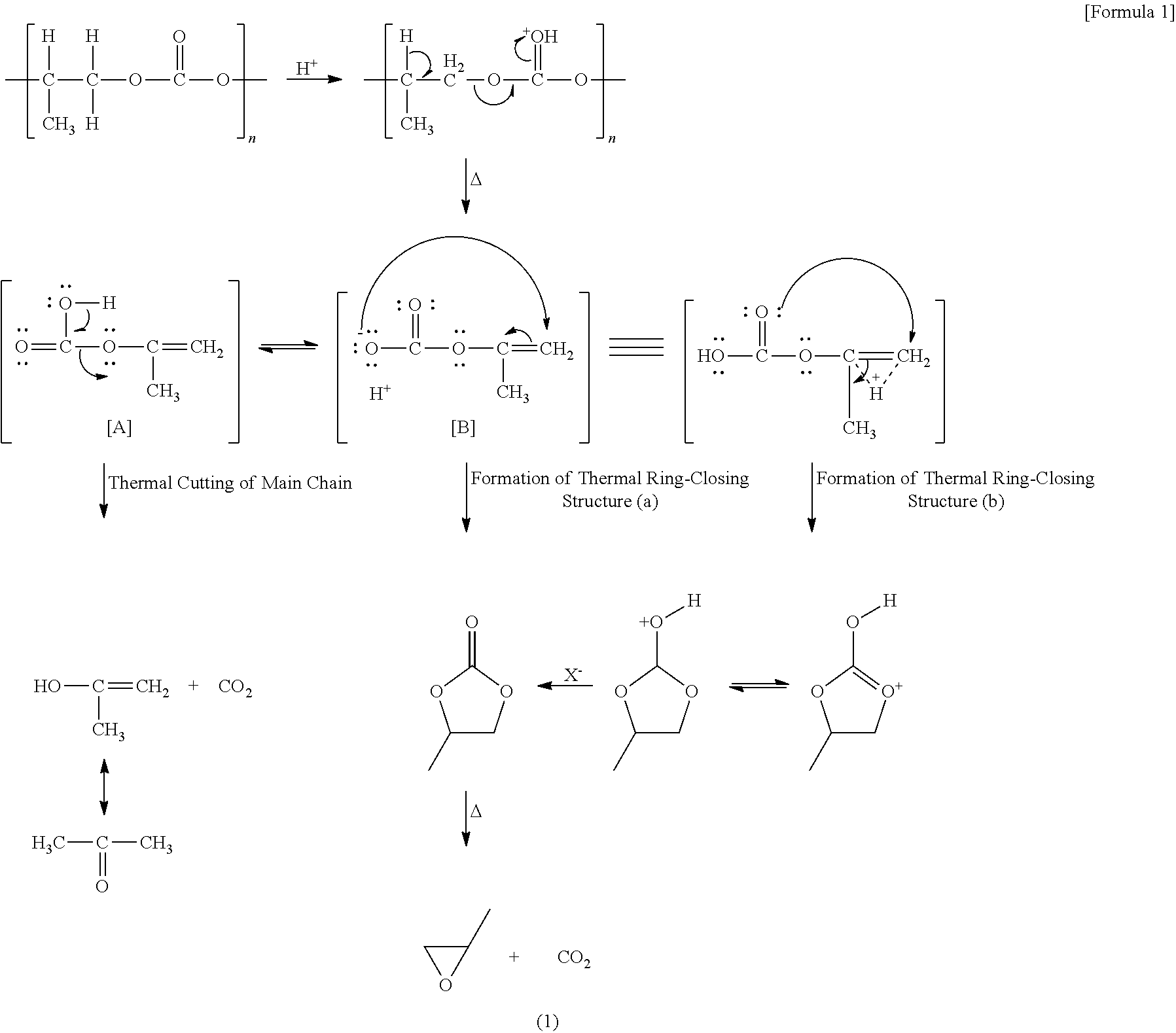
[0115]Herebelow, a detailed description of the temporary bonding adhesive for a semiconductor wafer, and a manufacturing method for a semiconductor device of the present invention, shall be explained using embodied examples, but the present invention is not limited to the embodied examples described below.

Production of Temporary Bonding Adhesive

embodiment 1

[0116]In Embodiment 1, a temporary bonding adhesive was produced using the following compound.

Synthesis of 1,4-polybutylane carbonate

[0117]In a three neck flask provided with an agitator, a raw material loading opening, and a nitrogen gas introduction opening, 1,4-butanediol (168 g, 1.864 mol) and diethyl carbonate (264.2 g, 2.236 mol) were added, heated to 90 to 100 degrees Celsius under a nitrogen atmosphere, and the mixture was dissolved. Next, after adding a 20% sodium ethoxide ethanol solution (80 ml, 0.186 mol), this was agitated for one hour at 90 to 100 degrees Celsius under a nitrogen atmosphere. After this, the interior of the reaction container was depressurized by around 30 kPa, and left at 90 to 100 degrees Celsius for 1 hour, and 120 degrees Celsius for 1 hour. After this, in a vacuum of 0.1 kPa, agitation was done for 1 hour at 150 degrees Celsius, and for 2 hours at 180 degrees Celsius.

[0118]The reactants obtained above were dissolved in tetrahydrofuran (2 L), filter...

embodiment 2

[0120]For Embodiment 2, a temporary bonding adhesive was produced using the following compound.

[0121]In a three neck flask provided with an agitator, a raw material loading opening, and a nitrogen gas introduction opening, neopentyl glycol (194.2 g, 1.864 mol) and diethyl carbonate (308.2 g, 2.610 mol) were added, heated to 120 degrees Celsius under a nitrogen atmosphere, and the mixture was dissolved.

[0122]Next, after adding a 20% sodium ethoxide ethanol solution (80 ml, 0.186 mol), this was agitated for 2 hours at 120 degrees Celsius under a nitrogen atmosphere. After this, the interior of the reaction container was depressurized by around 30 kPa, and agitated at 120 degrees Celsius for 1 hour. After this, in a vacuum of 0.1 kPa, agitation was done for 3 hours at 120 degrees Celsius.

[0123]The reactants obtained above were dissolved in tetrahydrofuran (2 L), filtering was done, and the catalysis residue was removed. After this, this filtered liquid was put into a distilled water:me...


PUM

PropertyMeasurementUnit
weight loss temperatureaaaaaaaaaa
thicknessesaaaaaaaaaa

Abstract

To provide a temporary bonding adhesive for a semiconductor wafer that reduces damage to a semiconductor wafer, makes it readily detachable, and can shorten the time required for thermal decomposition, and a manufacturing method for a semiconductor device using this.A temporary bonding adhesive for a semiconductor wafer, being a temporary bonding adhesive used for temporarily bonding a semiconductor wafer onto a supporting substrate in order to process a semiconductor wafer, and for detaching a semiconductor wafer from a supporting substrate by heating after processing, containing a resin composition composition whereof the 50% weight loss temperature decreases after irradiation by active energy rays.

Description

FIELD OF THE INVENTION[0001]The present invention concerns a temporary bonding adhesive for temporarily bonding a semiconductor wafer during processing, and a method for manufacturing a semiconductor device using the same, and use of a resin composition as a temporary bonding adhesive.BACKGROUND OF THE INVENTION[0002]In order to carry out processing such as grinding and etching on semiconductor wafers, it is necessary to temporarily bond semiconductor wafers, and various methods for doing so have been proposed. For example, at present, a method wherein a semiconductor wafer is bonded on top of a film for bonding that is a PET film whereon an adhesive layer has been provided is often used.[0003]With this method, if the grinding precision (approximately 1 μm) of a back grinding machine generally used for grinding, and the thickness precision (approximately 5 μm) of a BG (back grind) tape generally used to fix a wafer are put together, the required thickness precision is exceeded, and ...

Claims


Application Information

Patent Timeline
Patent Type & Authority Applications(United States)
IPC IPC(8): C09J169/00C08J3/28H01L21/302
CPCC09D177/00C09D179/08C09J169/00H01L2221/68386H01L21/6836H01L2221/68327H01L2221/6834H01L21/6835
Inventor TAKEUCHI, ETSUKUSUNOKI, JUNYASUGIYAMA, HIROMICHIKUBOYAMA, TOSHIHARUKAWATA, MASAKAZU
Owner SUMITOMO BAKELITE CO LTD
Why Eureka
Try Eureka