Driving method of liquid crystal display device

a liquid crystal display and driving method technology, applied in static indicating devices, instruments, digital data processing details, etc., can solve the problems of short continuous operation time and low power consumption, and achieve the effect of preventing the quality of the displayed image from being lowered, reducing power consumption, and increasing the aperture ratio

Inactive Publication Date: 2012-01-05
SEMICON ENERGY LAB CO LTD
View PDF5 Cites 27 Cited by
  • Summary
  • Abstract
  • Description
  • Claims
  • Application Information

AI Technical Summary

Benefits of technology

[0005]Low power consumption is one of the important points in terms of evaluating performance of a semiconductor display device, and a liquid crystal display device is no exception in that point. In particular, when a portable electronic device such as a cellular phone is used, large power consumption of a liquid crystal display device leads to a disadvantage of short continuous operation time; therefore, low power consumption is required.
[0006]In the case of a transmissive liquid crystal display device, if the percentage of a region transmitting light in a pixel, that is, the aperture ratio is increased, light emitted from a backlight can be efficiently utilized; accordingly, power consumption can be reduced. However, if priority is put on the increase in the aperture ratio when determining the pixel layout, the size of a semiconductor element such as a transistor or a capacitor included in the pixel needs to be reduced. When the capacitance of a capacitor is reduced, the period for which the potential of an image signal can be held is shortened; accordingly, the quality of the displayed image is lowered.
[0007]In consideration of the above-described problems, it is an object of an embodiment of the present invention to provide a driving method of a liquid crystal display device which can realize a reduction in the power consumption with the image quality prevented from being lowered.

Problems solved by technology

In particular, when a portable electronic device such as a cellular phone is used, large power consumption of a liquid crystal display device leads to a disadvantage of short continuous operation time; therefore, low power consumption is required.

Method used


Image

  • Driving method of liquid crystal display device
  • Driving method of liquid crystal display device
  • Driving method of liquid crystal display device

Examples


embodiment 1

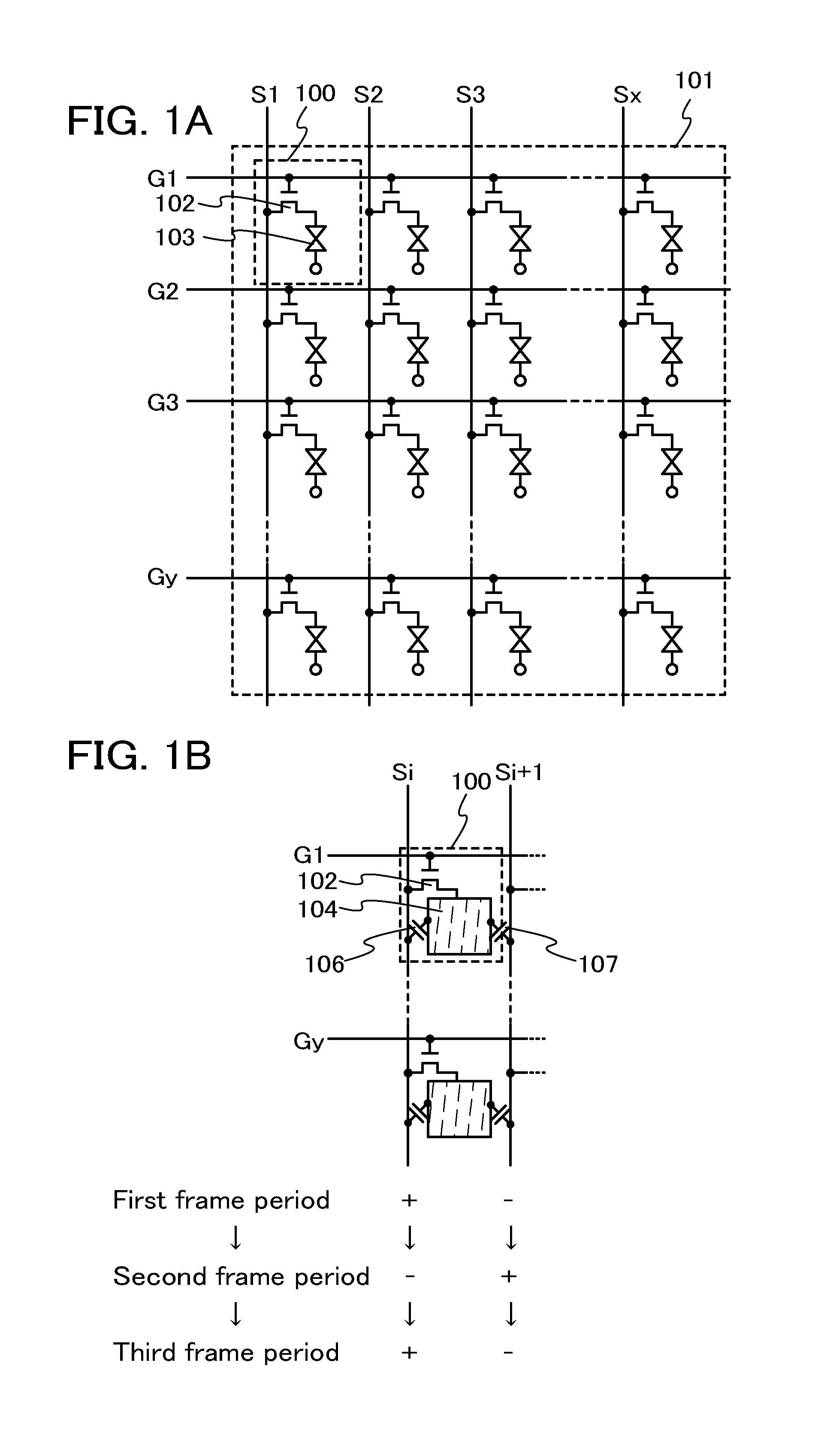
[0040]A liquid crystal display device used in a driving method according to an embodiment of the present invention includes a plurality of pixels, each of which is provided with a liquid crystal element and a transistor which controls supply of an image signal to the liquid crystal element. A plurality of scan lines for selecting the plurality of pixels and a plurality of signal lines for supplying image signals to the selected pixels are connected to the plurality of pixels.

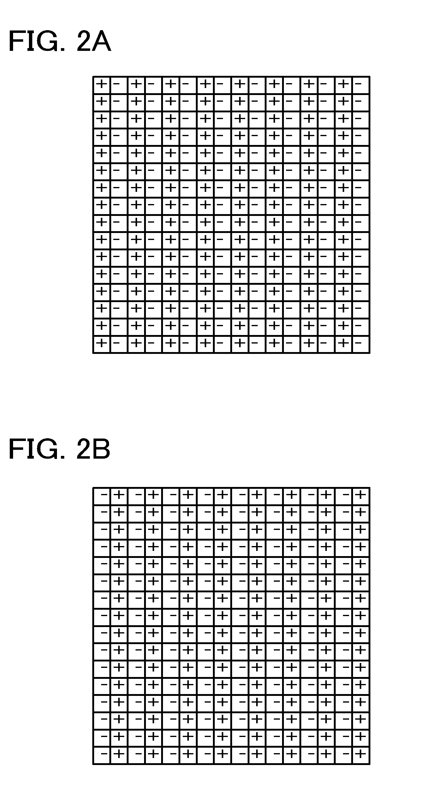
[0041]FIG. 1A illustrates a structure of a pixel portion 101 including a plurality of pixels 100, as an example. In FIG. 1A, each of the pixels 100 includes at least one of signal lines S1 to Sx and at least one of scanning lines G1 to Gy. In addition, the pixel 100 includes a transistor 102 which functions as a switching element and a liquid crystal element 103. The liquid crystal element 103 includes a pixel electrode, a counter electrode, and a liquid crystal to which voltage between the pixel electrode and t...

embodiment 2

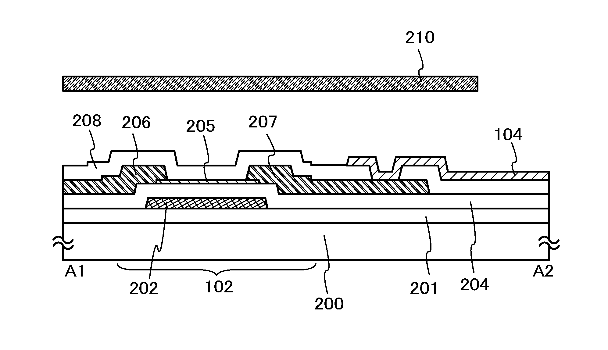
[0098]In this embodiment, a manufacturing method of a transistor including an oxide semiconductor will be described.

[0099]First, as illustrated in FIG. 6A, an insulating film 701 is formed over an insulating surface of a substrate 700, and a gate electrode 702 is formed over the insulating film 701.

[0100]Although there is no particular limitation on a substrate which can be used as the substrate 700 as long as it has a light-transmitting property, it is necessary that the substrate have at least enough heat resistance to heat treatment performed later. For example, a glass substrate manufactured by a fusion process or a float process, a quartz substrate, a ceramic substrate, or the like can be used as the substrate 700. When the temperature of the heat treatment performed later is high, a substrate having a strain point of 730° C. or higher is preferably used as the glass substrate. Although a substrate formed of a flexible synthetic resin such as plastic generally has a lower resis...

embodiment 3

[0156]In this embodiment, structural examples of a transistor will be described. Note that the same portions as those in the above embodiments and portions having functions similar to those in the above embodiments can be formed in a manner similar to that of the above embodiments. The same steps as those in the above embodiments and steps similar to those in the above embodiments can be conducted in a manner similar to those of the above embodiments. Therefore, the descriptions thereof are not repeated in this embodiment. In addition, detailed description of the same portion is not repeated, either.

[0157]A transistor 2450 illustrated in FIG. 7A includes a gate electrode 2401 over a substrate 2400, a gate insulating film 2402 over the gate electrode 2401, an oxide semiconductor film 2403 over the gate insulating film 2402, and a source electrode 2405a and a drain electrode 2405b over the oxide semiconductor film 2403. An insulating film 2407 is formed over the oxide semiconductor fi...


PUM


Abstract

An object is to provide a driving method of a liquid crystal display device with a low power consumption and a high image quality. A pixel includes a liquid crystal element and a transistor which controls supply of an image signal to the liquid crystal element. The transistor includes, in a channel formation region, a semiconductor which has a wider band gap than a silicon semiconductor and has a lower intrinsic carrier density than silicon, and has an extremely low off-state current. In inversion driving of pixels, image signals having opposite polarities are input to a pair of signal lines between which a pixel electrode is disposed. By employing such a structure, the quality of the displayed image can be increased even in the absence of a capacitor in the pixel.

Description

TECHNICAL FIELD[0001]The present invention relates to a driving method of an active-matrix liquid crystal display device including a transistor in a pixel.BACKGROUND ART[0002]In recent years, a metal oxide having semiconductor characteristics, which is called an oxide semiconductor, has attracted attention as a novel semiconductor material for a semiconductor element having high mobility provided by polysilicon or microcrystalline silicon and having uniform element characteristics provided by amorphous silicon. The metal oxide is used for various applications; for example, indium oxide is a well-known metal oxide and used as a material of a pixel electrode in a liquid crystal display device. Examples of such a metal oxide having semiconductor characteristics include tungsten oxide, tin oxide, indium oxide, and zinc oxide. Transistors in which a channel formation region is formed using such a metal oxide having semiconductor characteristics have been already known (Patent Documents 1...

Claims


Application Information

Patent Timeline
Patent Type & Authority Applications(United States)
IPC IPC(8): G06F3/038H01L29/02
CPCH01L27/1225G09G3/3648G09G3/3614G06F1/3265Y02D10/00G06F3/038H01L29/02
Inventor MIYAKE, HIROYUKISHISHIDO, HIDEAKIARASAWA, RYO
Owner SEMICON ENERGY LAB CO LTD
Why Eureka
Try Eureka