Methods and compositions for doping silicon substrates with molecular monolayers

a silicon substrate and monolayer technology, applied in the direction of basic electric elements, semiconductor/solid-state device manufacturing, electric devices, etc., can solve the problems of limiting the formation of sub-10 nm usjs by conventional technologies, affecting the use of ic manufacturing, and unable to solve problems, etc., to achieve rapid thermal annealing

Inactive Publication Date: 2012-01-05
VERSUM MATERIALS US LLC
View PDF1 Cites 23 Cited by
  • Summary
  • Abstract
  • Description
  • Claims
  • Application Information

AI Technical Summary

Benefits of technology

[0009]In one preferred embodiment of the present invention there is provided a method for doping a Si surface comprising treating the substrate with a diluted dopant solution comprising tetraethylene glycol dimethyl ether (tetraglyme) and a dopant-containing material and subsequently diffusing the dopant into the surface. Dithyl-1-propylphosphonate and allylboronic acid pinacol ester ...

Problems solved by technology

Unfortunately, point defects such as Si interstitials and vacancies are also generated, which interact with the dopants to further broaden the junction profile—called transient-enhanced diffusion (TED), which limits the formation for sub-10 nm USJs by conventional technologies.
However, problems relating to the effects of advanced doping and annealing techniques...

Method used


Image

  • Methods and compositions for doping silicon substrates with molecular monolayers
  • Methods and compositions for doping silicon substrates with molecular monolayers

Examples


example 1

Solubility Testing

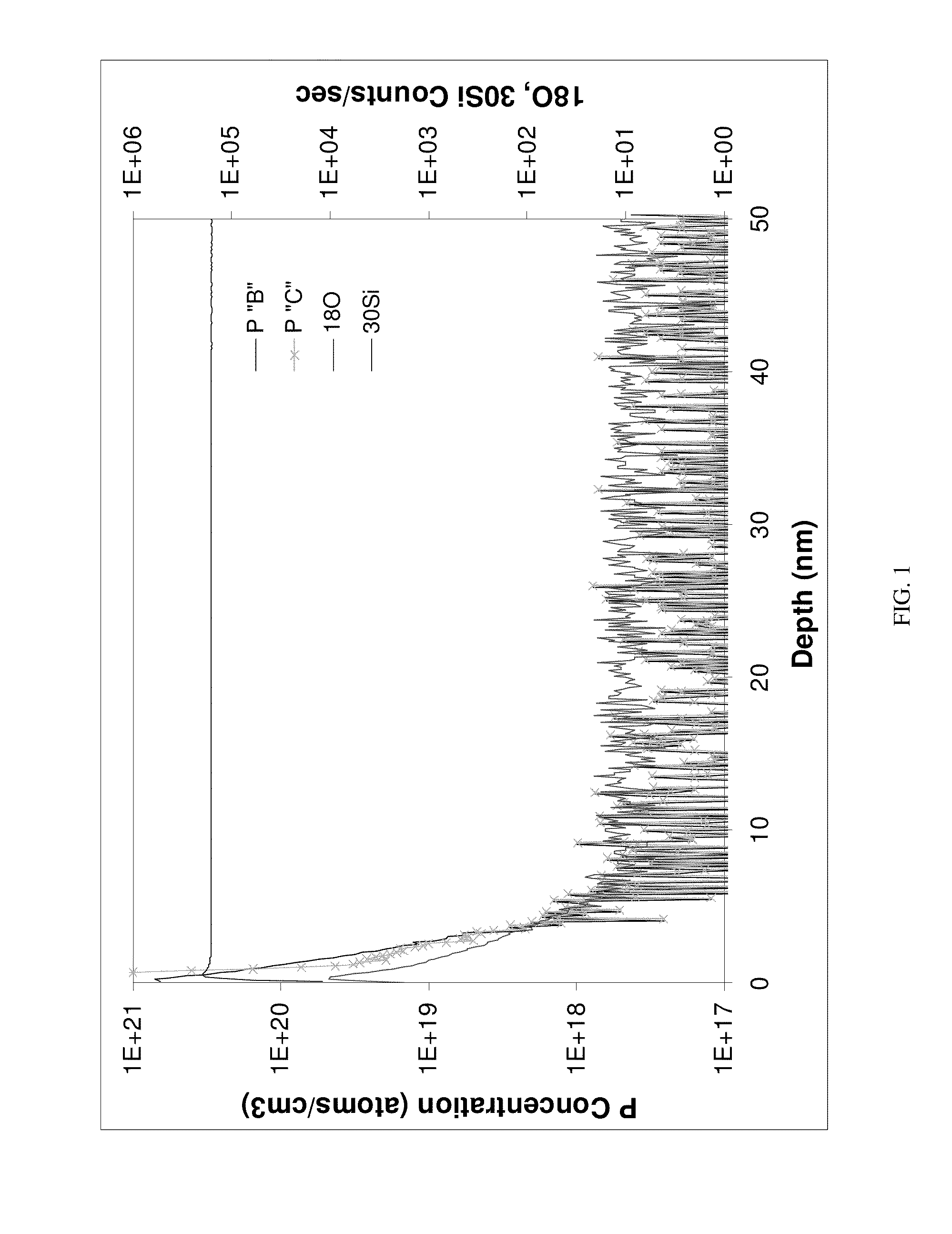
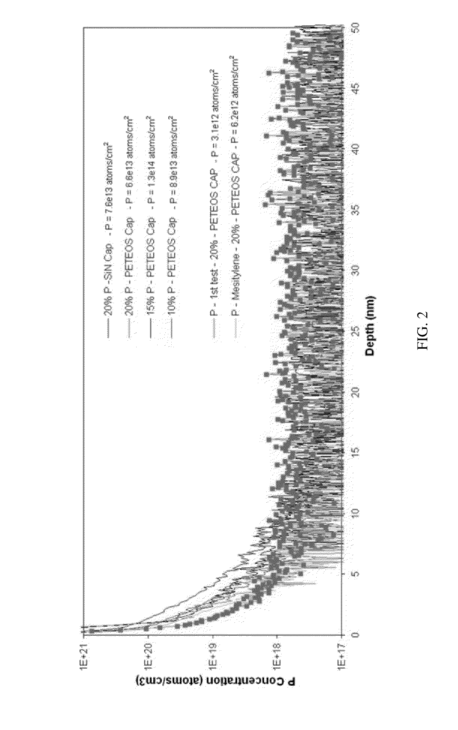
[0025]A variety of solvents were evaluated as potential replacements for mesitylene in allylboronic acid pinacol ester:mesitylene and diethylpropyl-phosphonate:mesitylene systems. The candidate solvents included: 1) Dimethylsulfoxide (DMSO); 2) N-methylpyrrolidone (NMP); 3) 1-formyl piperidine (1-FP); 4) tetraglyme, (TG); and 5) Isopar M (IM).

[0026]Solubility was tested with diethyl 1-propylphoshonate 97% (n-type dopant) and allylboronic acid pinacol ester (p-type dopant). Solvent to additive ratio (n or p type) material is 1:4. Solubility results are provided below:

Solvent and Diethyl 1-Solubility observations after 12 hrs, @propylphoshonate23° C.DMSOClear, stayed in sol'nNMPClear, stayed in sol'n1-FPClear, stayed in sol'nTGClear, stayed in sol'nIMClear, stayed in sol'n

Solvent and Allyboronic acidSolubility observations after 12 hrs,pinacol ester@ 23° C.DMSOSlightly cloudy, stayed in sol'nNMPSlightly cloudy, stayed in sol'n1-FPClear, stayed in sol'nTGClear, stayed...

example 2

Contact Angle Testing

[0028]Contact angle testing was also conducted. Silicon substrates (n-doped and p-doped prior to testing) were submerged in 0.5% HF(aq) for 2 minutes at room temperature (23° C.) before testing contact angles. DI water and mesitylene were used as references.

[0029]The observed contact angles on Si (100) n-type and p-type are reported below:

Solvent and Diethyl 1-propylphoshonateSubstrateContact AngleMesitylenen-doped SiNo reading = 0p-doped SiNo reading = 0DMSOn-doped SiNo reading = 0p-doped SiAvg. = 22.57°NMPn-doped SiNo reading = 0p-doped SiNo reading = 01-Formyl Piperidinen-doped SiNo reading = 0p-doped SiNo reading = 0Tetraglymen-doped SiNo reading = 0p-doped SiNo reading = 0Isopar Mn-doped SiNo reading = 0p-doped SiNo reading = 0

Solvent and Allylboronic acid pinacolesterSubstrateContact AngleMesitylenen-doped SiNo reading = 0p-doped SiNo reading = 0DMSOn-doped SiNo reading = 0p-doped SiNo reading = 0NMPn-doped SiNo reading = 0p-doped SiNo reading = 01-FPn-dop...

example 3

Phosphorus Doping

[0031]Diluted dopant solutions were used to dope a Si substrate. The following glassware was used for the doping testing: 3 neck round bottom flask (500 mL), 2 distilling columns, stainless steel tube for N2 inlet, 2 thermometer adaptors, Y distillation adaptor, 4 tubes for columns and N2, circulation bath, thermometer, heating mantel.

[0032]The following materials were used: N2 (ultra high purity), Ethylene Glycol / water mixture (1:1), experimental solution (solutions used are listed below), 3-methyoxy-3-methylbutanol, 0.5% HF solution, IPA, n-type Si substrate, p-type Si substrate.

[0033]The test procedure was as follows:

1. Set up the glassware, reflux bath (ethylene glycol and DI 1:1), place round bottom flask on heating mantel, cleave Si substrate into small pieces about 1½ cm×1½ cm for testing. Both n- and p-type substrates were processed at the same time.

2. Prepare Solutions:

[0034]HF (0.5% in solution)[0035]3-methoxy-3-methylbutanol[0036]Experimental solution:[00...


PUM


Abstract

Compositions and methods for doping silicon substrates by treating the substrate with a diluted dopant solution comprising tetraethylene glycol dimethyl ether (tetraglyme) and a dopant-containing material and subsequently diffusing the dopant into the surface by rapid thermal annealing. Diethyl-1-propylphosphonate and allylboronic acid pinacol ester are preferred dopant-containing materials, and are preferably included in the diluted dopant solution in an amount ranging from about 1% to about 20%, with a dopant amount of 4% or less being more preferred.

Description

[0001]This application claims priority from U.S. Provisional Patent Application No. 61 / 311,516, filed Mar. 8, 2010, the entire contents of which is hereby incorporated herein by reference.FIELD OF THE INVENTION[0002]The present invention relates generally to methods for doping a Si surface, and more particularly to methods for doping a Si surface by treating the substrate with a dopant solution and subsequently diffusing the dopant into the surface by rapid thermal annealing.BACKGROUND OF THE INVENTION[0003]Decreasing device size has been the main driving force for technology advancements in the semiconductor industry over the last several decades. For example, in front end of line (FEOL) applications in semiconductor processing, junction depths have been scaled continuously together with the gate lengths in order to achieve faster transistor speeds and higher packing densities. Typically, source / drain extension junction depths of about one third of the transistor gate length have b...

Claims


Application Information

Patent Timeline
IPC IPC(8): H01L21/22
CPCH01L21/2225H01L21/228H01L21/2254H01L21/02052H01L21/02057H01L21/02123H01L21/2686H01L21/388H01L21/02623
Inventor POLLARD, KIMBERLY DONARECTOR, ALLISON C.
Owner VERSUM MATERIALS US LLC
Why Eureka
Try Eureka