High-Efficiency, Monolithic, Multi-Bandgap, Tandem, Photovoltaic Energy Converters

a photovoltaic and solar energy converter technology, applied in the field of monolithic, multi-bandgap, tandem photovoltaic solar energy converters, can solve the problems of reducing energy conversion efficiency, inefficiency and energy loss to unwanted heat, and knowledge alone cannot solve the problem of making efficient and useful energy conversion devices, etc., to achieve special usefulness, avoid defects in lattice-mismatched layers, and improve efficiency

a photovoltaic and solar energy converter technology, applied in the field of monolithic, multi-bandgap, tandem photovoltaic solar energy converters, can solve the problems of reducing energy conversion efficiency, inefficiency and energy loss to unwanted heat, and knowledge alone cannot solve the problem of making efficient and useful energy conversion devices, etc., to achieve special usefulness, avoid defects in lattice-mismatched layers, and improve efficiency

US20120015469A1Inactive Publication Date: 2012-01-19ALLIANCE FOR SUSTAINABLE ENERGY

Image

  • High-Efficiency, Monolithic, Multi-Bandgap, Tandem, Photovoltaic Energy Converters
  • High-Efficiency, Monolithic, Multi-Bandgap, Tandem, Photovoltaic Energy Converters
  • High-Efficiency, Monolithic, Multi-Bandgap, Tandem, Photovoltaic Energy Converters

Examples


examples

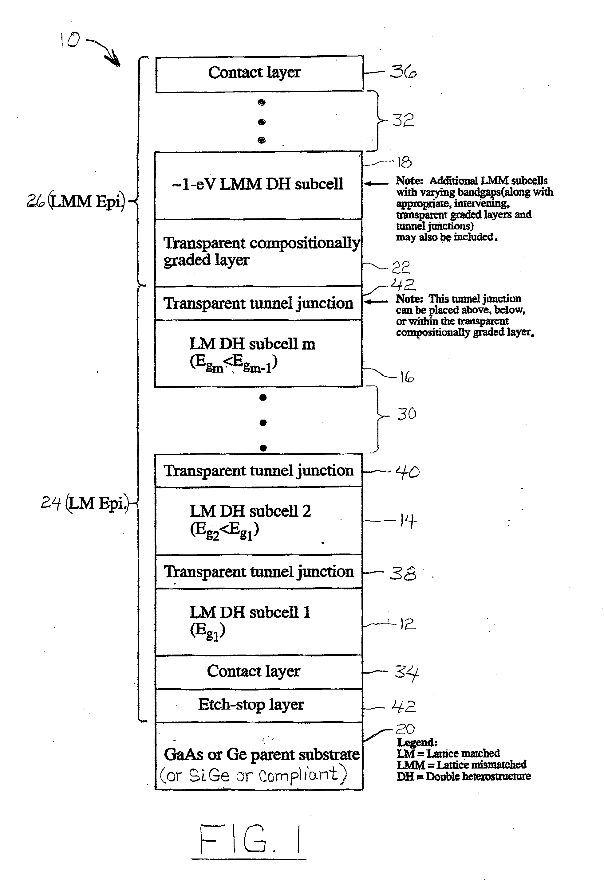
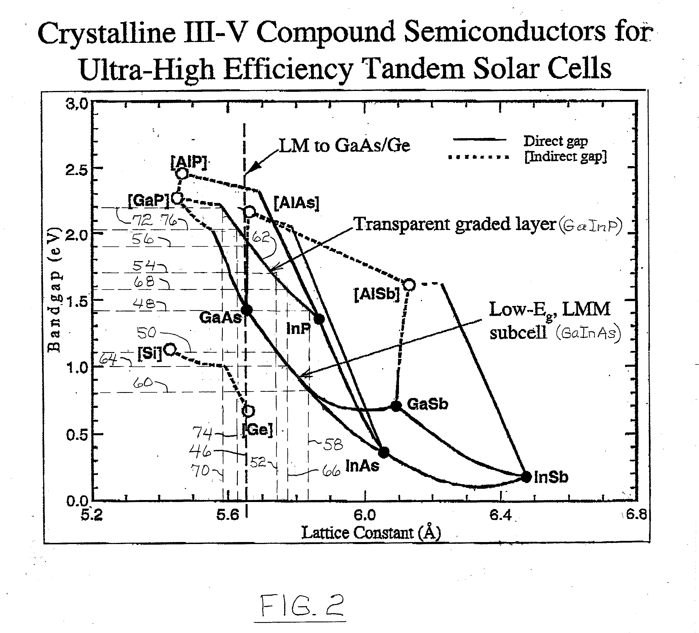
[0060]A series-connected, three-subcell device was grown on a GaAs substrate. LM n-GaInP {1 μm) etch-stop and n-GaAs (0.4 μm) contact layers were grown first. A LM DH top subcell comprising an n-AlInP (25 nm) front-surface confinement layer (FSCL), n-GaInP (0.1 μm, ordered) emitter layer, p-GaInP (1.2 μm, ordered) base layer, and a p-GaInP (0.1 μm, disordered) back-surface confinement layer (BSCL) was then deposited, followed by a p+ / n+ GaAs tunnel junction (24 nm total thickness). The LM middle subcell comprises a n-GaInP (0.1 μm) emitter layer, a p-GaAs (2.5 μm) base layer, and a p-GaInP (50 nm, ordered) BSCL, followed by another p+ / n+ GaAs tunnel junction (24 nm total thickness). A transparent, compositionally step-graded GaInP layer was then grown to affect a change in lattice constant to match that of the low bandgap (˜1 eV) GaInAs alloy (Ga mole fraction of 0.75, LMM ˜2.2%). The step grade included nine compositional steps with a Ga mole fraction increment of 0.03 per step, an...


PUM


Abstract

A monolithic, multi-bandgap, tandem solar photovoltaic converter has at least one, and preferably at least two, subcells grown lattice-matched on a substrate with a bandgap in medium to high energy portions of the solar spectrum and at least one subcell grown lattice-mismatched to the substrate with a bandgap in the low energy portion of the solar spectrum, for example, about 1 eV.

Description

CROSS-REFERENCE TO RELATED APPLICATIONS[0001]This application is a continuation-in-part of U.S. patent application Ser. No. 10 / 515,243, entitled “Low-Bandgap, Monolithic, Multi-Bandgap, Optoelectronic Devices,” filed on Nov. 19, 2004, which is incorporated herein by reference for all that it discloses.CONTRACTUAL ORIGIN OF THE INVENTION[0002]The United States Government has rights in this invention under Contract No. DE-AC36-99GO10337 between the United States Department of Energy and the National Renewable Energy Laboratory, a Division of the Midwest Research Institute.TECHNICAL FIELD[0003]This invention is related to photovoltaic devices and, more specifically, to monolithic, multi-bandgap, tandem photovoltaic solar energy converters.BACKGROUND OF THE INVENTION[0004]It is well-known that the most efficient conversion of solar energy to electrical energy with the least thermalization loss in semiconductor materials is accomplished by matching the photon energy of the incident solar...

Claims


Application Information

Patent Timeline
19 Jan 2012
Publication
US20120015469A1
IPC
H01L31/18
CPC
H01L31/06875; H01L31/046; Y02E10/544; H01L31/0687; H01L31/043; H01L31/0475
Inventors
WANLASS, MARK W.