Method of Producing Stable Oxygen Terminated Semiconducting Nanoparticles

a technology of semiconducting nanoparticles and oxygen, which is applied in the direction of arsenic compounds, cell components, gas-gas reaction processes, etc., can solve the problems of high technology options, unstable undecorated silicon surfaces, and high cost of nanotechnology

Inactive Publication Date: 2012-01-26
PST SENSORS
View PDF0 Cites 4 Cited by
  • Summary
  • Abstract
  • Description
  • Claims
  • Application Information

AI Technical Summary

Benefits of technology

[0011]A stable stoichiometric oxide of one or more component elements of the semiconductor material may be reduced, or prevented from forming, by a preferential chemical reaction.
[0012]Alternatively, an intermediate sub-stoichiometric oxide of one or more component elements of the semiconductor material may be reduced, or prevented from forming, by a preferential chemical reaction, thus hindering the formation of the final stable stoichiometric phase of the oxide.

Problems solved by technology

In basic scientific studies a stable, well characterised surface is required, which has led to nanotechnology being seen as an expensive, high technology option, with complex synthesis and handling techniques.
Bare, undecorated silicon surfaces are only stable under ultra high vacuum conditions.

Method used


Image

  • Method of Producing Stable Oxygen Terminated Semiconducting Nanoparticles
  • Method of Producing Stable Oxygen Terminated Semiconducting Nanoparticles
  • Method of Producing Stable Oxygen Terminated Semiconducting Nanoparticles

Examples


example 1

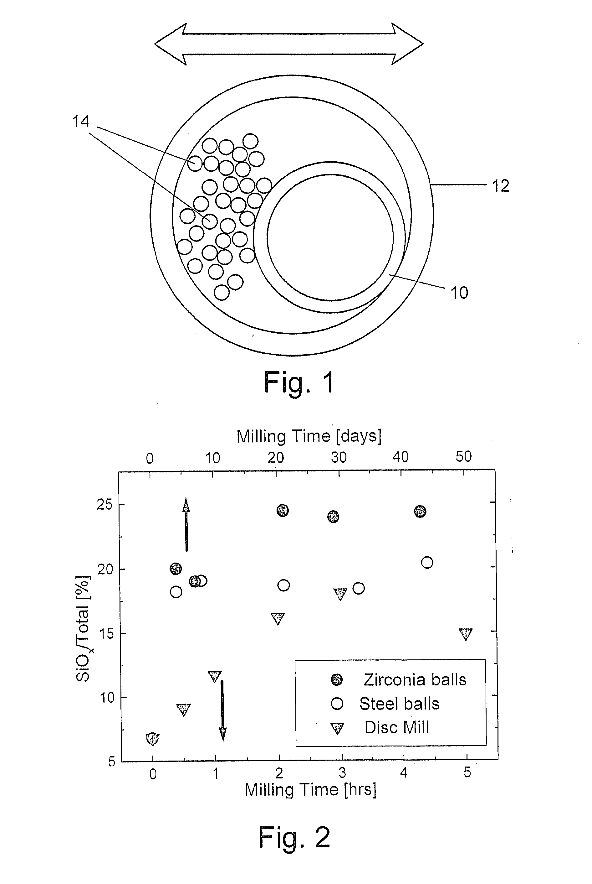
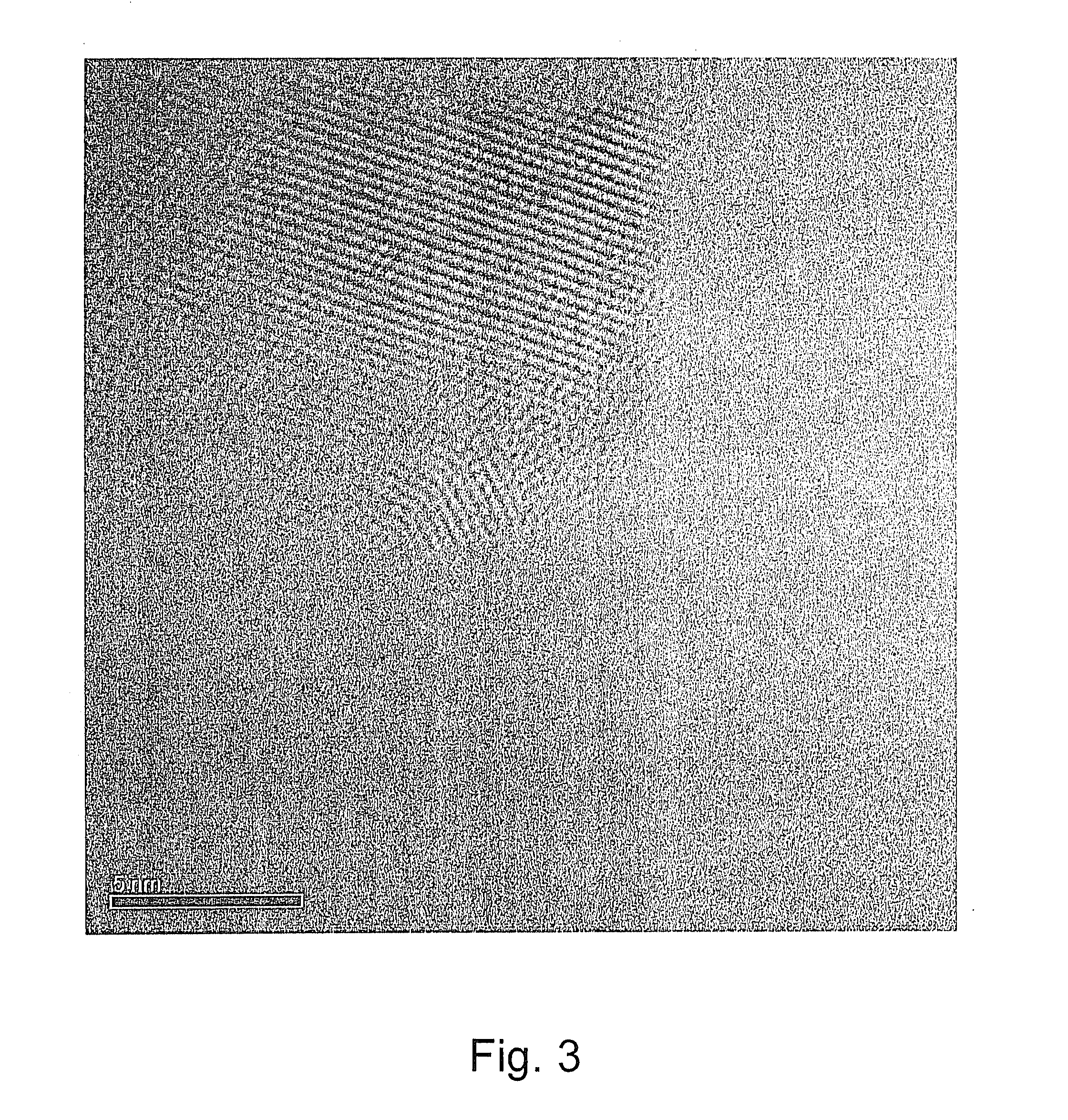
[0053]The methods as envisaged in the first two embodiments have been applied using 51200 chrome steel milling media. As a reference material, a bulk material comprising 2503 grade silicon metal was dry milled, at room temperature, for extended periods in a laboratory ball mill with a neoprene drum, using zirconia balls as the milling media. Following established procedures, as the particle size was reduced, the size of the zirconia balls was reduced from 15 mm diameter, through 10 mm, to 5 mm.

[0054]In accordance with the first embodiment of the method, 2503 grade silicon metal was milled, in air, for periods up to five hours, in 30 minute intervals in a laboratory disc mill equipped with a 51200 chrome steel pestle and mortar. The temperature range was maintained between 100 and 160° C.

[0055]In accordance with the second embodiment, the same ball mill as used for milling the reference material was used to mill 2503 grade silicon metal, but using 15 mm diameter chrome steel balls as...


PUM

PropertyMeasurementUnit
temperatureaaaaaaaaaa

Abstract

A method is provided of producing inorganic semiconducting nanoparticles having a stable surface. The method comprises providing an inorganic bulk semiconductor material, such as silicon or germanium, and milling the bulk semiconductor material in the presence of a selected reducing agent. The reducing agent acts to chemically reduce oxides of one or more component elements of the semiconductor material, or prevent the formation of such oxides by being preferentially oxidised, thereby to provide semiconducting nanoparticles having a stable surface which allows electrical contact between the nanoparticles. The milling may take place in a mill in which the milling media and/or one or more components of the mill comprise the selected reducing agent. For example, the milling can be carried out in a high energy mill with a hammer action in which a pestle of the mill, a mortar of the mill, or both are composed of the selected reducing agent, or a low energy, stirred media mill, such as a ball mill, a rod mill or similar, in which the milling media, a lining of the mill, or both are composed of the reducing agent. The milling media or mill are typically composed of a metal selected from the group comprising iron, chromium, cobalt, nickel, tin, titanium, tungsten, vanadium, and aluminium, or an alloy containing one or more of said metals. In another embodiment of the method, the selected reducing agent comprises a liquid contained in the mill during milling of the bulk semiconductor material. The liquid is typically an acidic solution containing any of hydrochloric, sulphuric, nitric, acetic, formic, or carbonic acid, or a mixture thereof. The invention extends to a mill for carrying out the method.

Description

BACKGROUND OF THE INVENTION[0001]THIS invention relates to a method of producing inorganic semiconducting nanoparticles having a stable surface.[0002]Semiconductor nanoparticles, with a characteristic size of a few nanometres up to several hundred nanometres, are a widely studied type of material, in which size effects dominate over properties of the bulk material. Depending on the application, single particles may be dispersed randomly in a matrix (quantum dots, OLEDs. DSC cells, organic semiconducting inks); regularly arranged (photonic arrays); or form an interconnecting structure (inorganic semiconducting inks). The latter may be a close packed structure, random network or a fractal agglomeration of different sized clusters.[0003]In basic scientific studies a stable, well characterised surface is required, which has led to nanotechnology being seen as an expensive, high technology option, with complex synthesis and handling techniques. Bare, undecorated silicon surfaces are only...

Claims


Application Information

Patent Timeline
Patent Type & Authority Applications(United States)
IPC IPC(8): B02C23/00C01B33/02C01G21/21B01J19/00C01B19/04B82Y30/00B82Y40/00
CPCB02C17/00B02C17/20C22C1/0491C09K11/883B02C23/06B22F9/20B22F2009/041B22F2009/043B22F2009/049B22F2999/00C01B19/002C01B19/007C01B33/02C01B33/113C01G21/21C01G28/00C01G30/00C01P2002/82C01P2004/04C01P2006/40C09K11/62C09K11/668C09K11/70C09K11/74C09K11/75C09K11/881B22F9/04C22C1/047
Inventor BRITTON, DAVID THOMASHARTING, MARGIT
Owner PST SENSORS
Why Eureka
Try Eureka