Surface mounted LED packaging structure and method based on a silicon substrate

a technology of led packaging and silicon substrate, which is applied in the direction of semiconductor/solid-state device manufacturing, semiconductor devices, electrical devices, etc., can solve the problems of difficult miniaturization, poor heat resistance, and non-ideal heat dissipation, and achieve good thermal performance and low cost

Inactive Publication Date: 2012-02-02
APT ELECTRONICS
View PDF2 Cites 36 Cited by
  • Summary
  • Abstract
  • Description
  • Claims
  • Application Information

AI Technical Summary

Benefits of technology

[0006]The object of the invention is to overcome the shortcomings and deficiencies of prior art to provide a surface mounted LED structure with good thermal performance, process simplicity, low cost and controllable quality
[0016]Compared to prior art, the packaging structure of the present invention has good heat dissipation effect and small volume; meanwhile packaging without gold wires makes the structure highly reliable. The LED chip is directly flip-chip mounted in the surface of the silicon substrate without the step of digging deep grooves in the silicon wafer surface, thereby reducing process costs and process difficulty. Meanwhile, the LED chip can be easily arranged in the upper surface of the silicon wafer, and the connection and package of multi-chip modules can be achieved arbitrarily and conveniently. A method of fabricating the annular convex wall on the upper surface of the silicon wafer is used to achieve the formation of better lenses directly by package dispensing, with lower cost than traditional molded lenses.

Problems solved by technology

However, there are the following problems with this present surface mounted LED structure: because the packaging bracket 100 is formed by a metal bracket being used as the substrate and then being cut after a colloid is encapsulated by means of plastic injection grooves or molded shape, it results in poor heat resistance, non-ideal heat dissipation and difficult miniaturization.
Moreover, because the upper surface of the LED chip 200 is mounted and the structure of gold wires 300 for connecting electrodes is used, the connection failure of gold wires is often the failure mode mostly occurred during the production and use of LED.
In addition, the upper surface mounted LED chip 200 dissipates heat through sapphire and thus has poor heat dissipation effect.
At present, the products of SMD structure based on the silicon substrate still cannot enjoy mass sales and applications in practice, and only some related patents are reported.
It is required to dig a large and deep groove on the upper surface the silicon wafer and to subject the silicon wafer to corrosion for a long time, with the process complex and the cost higher.
Simultaneously with the groove deep, the difficulty in its internal wiring is increased.
Especially if the flip chip is used, it is required to make metal bumps on the electrode of the groove.
Furthermore, because there is the deep groove on the upper surface of the silicon substrate, it is not easy to integrate LED's peripheral circuits (such as anti-static protection circuit, driver circuit, etc.) in the silicon substrate, with the application prospects limited.
In addition, the number of chips placed in the groove is limited by the size of the groove, thereby not easy to achieve multi-chip modules.

Method used


Image

  • Surface mounted LED packaging structure and method based on a silicon substrate
  • Surface mounted LED packaging structure and method based on a silicon substrate
  • Surface mounted LED packaging structure and method based on a silicon substrate

Examples


Embodiment Construction

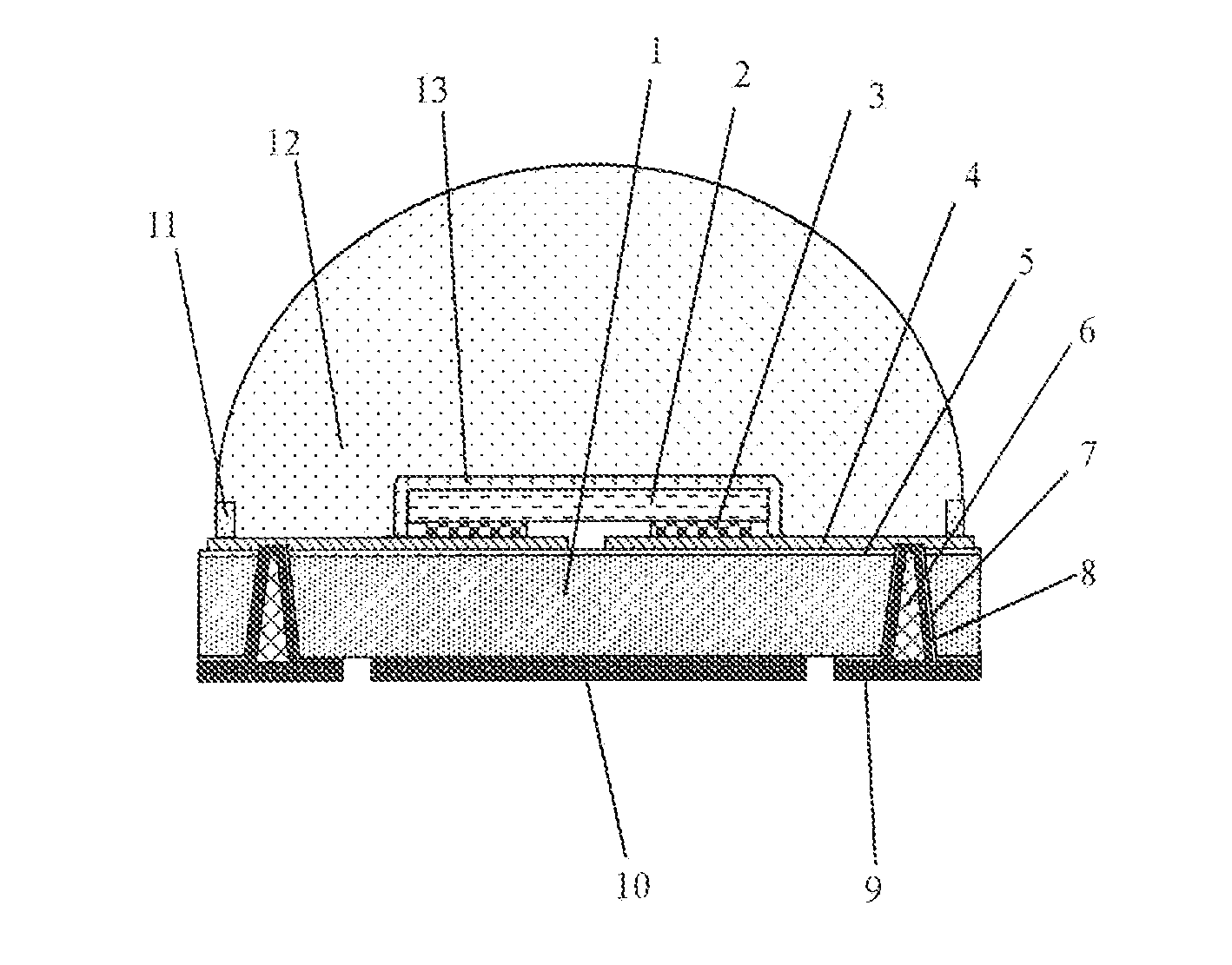
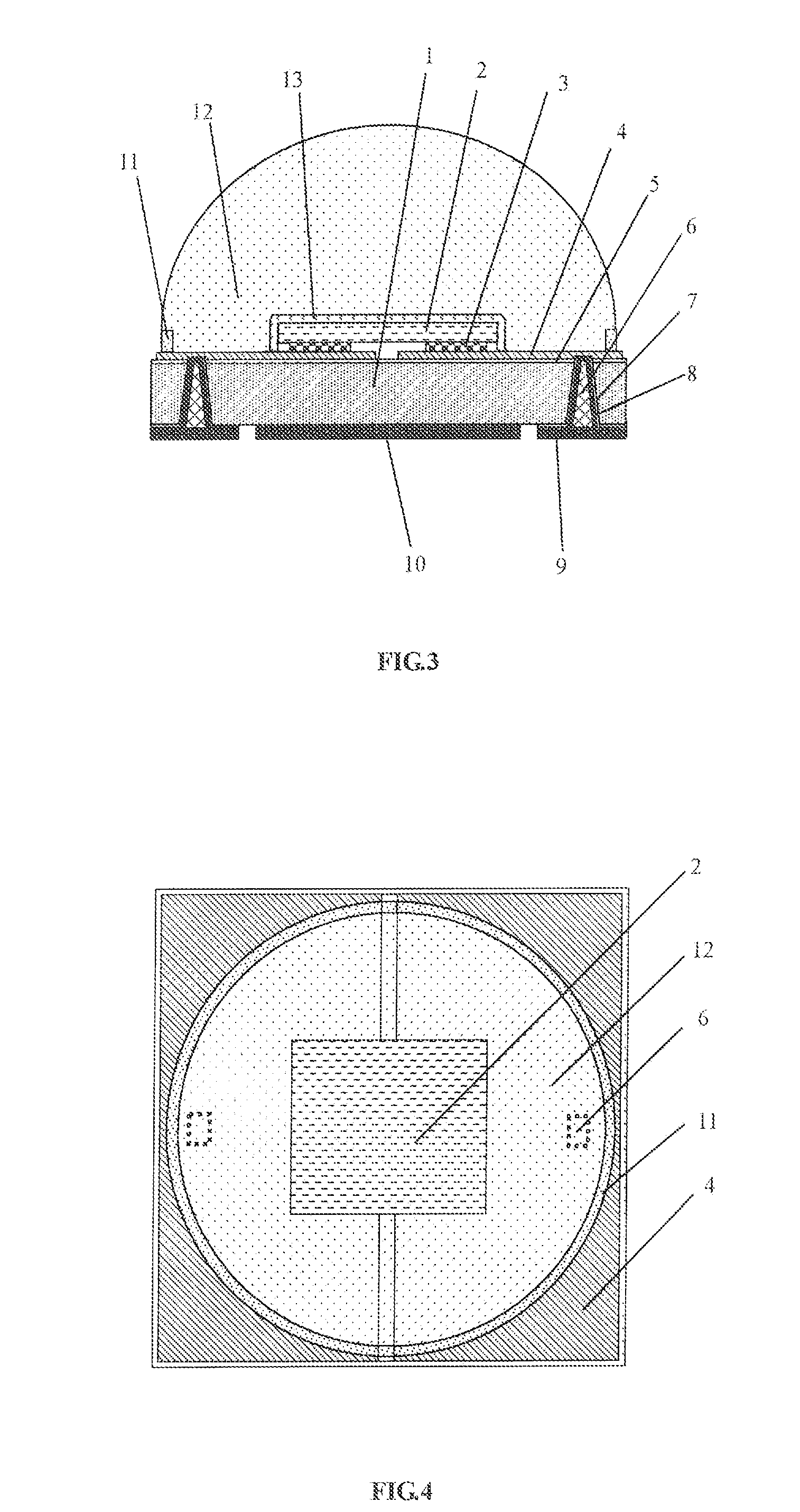
[0023]Now refer to FIGS. 3, 4 and 5, which are cross-section schematic view, top view and bottom view of the LED packaging structure based on the silicon substrate of the present invention, respectively. The LED packaging structure includes the silicon substrate 1, an LED chip 2 and a lens 12. In particular, the silicon substrate 1 has an upper surface of planar structure and without grooves. The upper surface of the silicon substrate 1 is covered by an oxide layer 5. Two metal electrode layers 4 for connecting positive and negative electrodes respectively are arranged in the upper surface of the oxide layer 5 and insulated from each other. The upper surfaces of the metal electrode layers 4 are respectively arranged with metal bumps 3. The LED chip 2 is flip-chip mounted on the silicon substrate 1, and the positive and negative electrodes of the LED chip 2 are respectively connected to the metal bumps 3 and thus connected to the metal electrode layers 4. Vias 6 through the upper and...


PUM

PropertyMeasurementUnit
heightaaaaaaaaaa
heightaaaaaaaaaa
insulatingaaaaaaaaaa

Abstract

A surface mounted LED packaging structure based on a silicon substrate includes the silicon substrate, an LED chip, an annular convex wall and a lens. The silicon substrate has an upper surface of planar structure and without grooves. An oxide layer covers the upper surface of the silicon substrate. Metal electrode layers are arranged in the upper surface of the oxide layer, and the upper surfaces of the metal electrode layers are arranged with metal bumps. Vias through the silicon substrate are provided under the metal electrode layers. An insulating layer covers the inner wall of the vias and a part of the lower surface of the silicon substrate. A metal connection layer covers the insulating layer surface within the vias. Two conductive metal pads are respectively arranged under the lower surface of the silicon substrate and insulated from the silicon substrate. A heat conduction metal pad is arranged on the lower surface of the silicon substrate. The LED chip is flip-chip mounted on the silicon substrate. The annular convex wall and the lens cause the LED chip and the metal electrode layers therein to be isolated from environment. The structure of the present invention has its advantages of good heat dissipation effect and small volume, while packaging without gold wires makes the structure highly reliable and achieves large-scale production of wafer level, resulting in the reduction of the packaging cost.

Description

CROSS-REFERENCE TO RELATED APPLICATION[0001]The present application claims priority of Chinese Patent Application CN201010243383.7 filed Jul. 30, 2010, the entire contents of which is incorporated herein by reference.FIELD OF THE INVENTION[0002]The present invention belongs to the field of manufacturing a light emitting device, and relates to an LED packaging structure and method based on a silicon substrate.BACKGROUND OF THE INVENTION[0003]The light emitting diode (LED) source has several advantages of high efficiency, long life and no harmful substances such as Hg and the likes. With the rapid development of LED technology, the LED's properties, such as brightness, lifetime and the likes, have been greatly improved, such that it has found an increasing application in a variety of areas ranging from outdoor lighting such as street lamps to indoor lighting such as decorative lights, in which LED is used or replaced as a light source.[0004]The LED packaging structure of surface mount...

Claims


Application Information

Patent Timeline
Patent Type & Authority Applications(United States)
IPC IPC(8): H01L33/58
CPCH01L33/486H01L33/54H01L2924/10253H01L2224/73265H01L2224/48227H01L2224/32225H01L2224/45144H01L33/64H01L33/62H01L2224/48091H01L2924/00014H01L2924/00
Inventor XIAO, GUOWEI DAVIDZENG, ZHAOMINGCHEN, HAIYINGZHOU, YUGANGHOU, YU
Owner APT ELECTRONICS
Why Eureka
Try Eureka