Supercharge Your Innovation With Domain-Expert AI Agents!

Cleaning sheet, transfer member with cleaning function, cleaning method of substrate processing apparatus, and substrate processing apparatus

a technology of transfer member and cleaning function, which is applied in the direction of cleaning equipment, film/foil adhesive, carpet cleaner, etc., can solve the problems of insufficient removal of foreign matter, reduced operation rate of processing apparatus, and large amount of time and labor for cleaning apparatus, etc., to achieve excellent foreign matter removal performance and transfer performance

Inactive Publication Date: 2012-02-23
NITTO DENKO CORP
View PDF5 Cites 9 Cited by
  • Summary
  • Abstract
  • Description
  • Claims
  • Application Information

AI Technical Summary

Benefits of technology

The present invention provides a cleaning sheet and a transfer member with a cleaning function that have excellent foreign matter removing performance and transfer performance. The cleaning sheet and transfer member can remove foreign matters each having a predetermined particle diameter with particularly high efficiency. The cleaning sheet and transfer member can be used to clean a substrate processing apparatus without stopping it, which solves the problem of decreased operation rate of the processing apparatus and the need for a great amount of time and labor for cleaning. The cleaning sheet and transfer member have a unique cleaning layer that has an uneven surface roughness and low adhesion to the substrate and transfer system, ensuring secure transfer of substrates and minimal damage to the transfer system. The cleaning sheet and transfer member can be easily attached and detached from the substrate processing apparatus. The method of cleaning a substrate processing apparatus using the cleaning sheet or transfer member of the present invention is simple and effective.

Problems solved by technology

In various kinds of substrate processing apparatuses that are apt to be easily damaged by foreign matter, such as a production apparatus and an inspection apparatus of a semiconductor, a flat panel display, and a printed board, each transfer system and substrate are transferred while they are brought into contact with each other.
As a result, there arise problems in that the operation rate of the processing apparatus decreases, and that a great amount of time and labor are required for cleaning the apparatus.
However, according to this method, foreign matter cannot be removed sufficiently.
Therefore, this method solves the problem in that the operation rate of the processing apparatus decreases and the problem in that a great amount time and labor are required for cleaning the apparatus.
Consequently, there arise problems in that the substrate may not be transferred securely, and that a transfer apparatus may be damaged.
In recent years, along with an increase in fineness of a semiconductor device, the adhesion of foreign matter to a wafer back surface as well as a wafer front surface has become a problem.
This is because the foreign matter transfers from the wafer back surface to the wafer front surface during a cleaning step, which decreases a production yield.
At present, a semiconductor element with a line width (design rule) of 65 nm is mainstream, and when a foreign matter of a size equal to or larger than the line width adheres to the semiconductor element, a defect such as open is liable to occur.
In particular, foreign matter having a particle diameter of about 0.2 to 2.0 μm is a problem.
However, any of the conventional technologies are insufficient for removing foreign matter each having a predetermined particle diameter with particularly high efficiency.

Method used


Image

  • Cleaning sheet, transfer member with cleaning function, cleaning method of substrate processing apparatus, and substrate processing apparatus
  • Cleaning sheet, transfer member with cleaning function, cleaning method of substrate processing apparatus, and substrate processing apparatus
  • Cleaning sheet, transfer member with cleaning function, cleaning method of substrate processing apparatus, and substrate processing apparatus

Examples


example 1

[0088]200 parts of polyethylene glycol 200 dimethacrylate (NK ester 4G (trade name) manufactured by Shin-Nakamura Chemical Co., Ltd.), 3 parts of a polyisocyanate compound (COLONATE L (trade name) manufactured by Nippon Polyurethane Industry Co., Ltd.), and 3 parts of benzyl dimethyl ketal (IRGACURE 651 (trade name) as a photopolymerization initiator, manufactured by Ciba Specialty Chemicals Holding Inc.) were mixed homogeneously with respect to 100 parts of an acrylic polymer (weight average molecular weight: 700,000) obtained from a monomer mixture solution formed of 75 parts of 2-ethylhexyl acrylate, 20 parts of methyl acrylate, and 5 parts of acrylic acid, thereby preparing a UV-curable pressure-sensitive adhesive solution A.

[0089]On the other hand, to a 500-ml three-necked flask reactor equipped with a thermometer, a stirrer, a nitrogen introducing tube, and a reflux condenser tube, 73 parts of 2-ethylhexyl acrylate, 10 parts of n-butyl acrylate, 15 parts of N,N-dimethylacrylam...

example 2

[0104]In an atmosphere of a nitrogen stream, 14.8 g of polyether diamine (XTJ-510 manufactured by Suntechno Chemical Co.), 8.45 g of 4,4′-DPE (DDE), and 10.0 g of pyromellitic dianhydride (PMDA) were mixed with 133 g of N,N-dimethylacetamide (DAMc) at 70° C. and allowed to react to obtain a polyamic acid solution A.

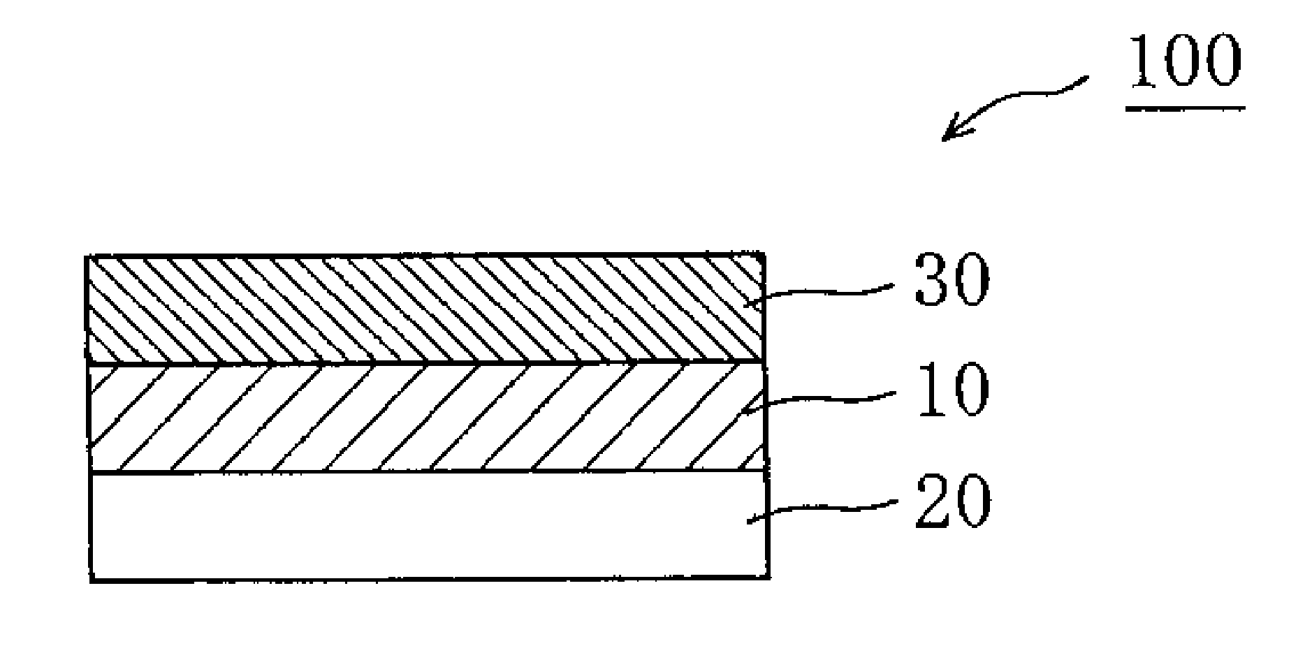
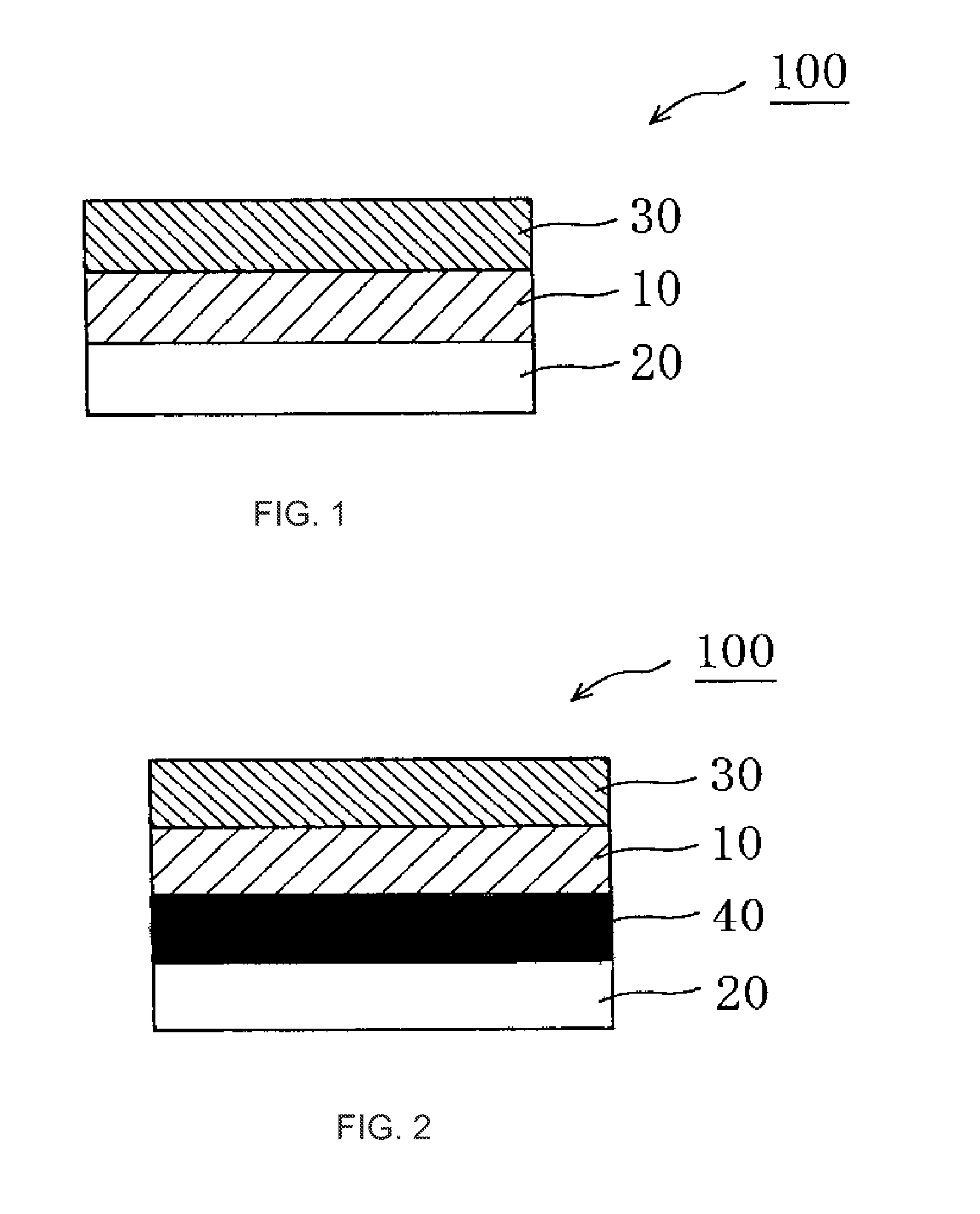
[0105]After being cooled, the polyamic acid solution A was applied onto an etching surface of an 8-inch silicon wafer with a spin coater and dried at 90° C. for 20 minutes to obtain a transfer member with polyamic acid (2).

[0106]The transfer member with polyamic acid (2) was heat-treated at 300° C. for 2 hours in an atmosphere of nitrogen to form a polyimide coating film with a thickness of 30 μm, and thus, a transfer member with a cleaning function (2) was obtained.

[0107]The average surface roughness Ra of the cleaning layer of the transfer member provided with a cleaning function (2) was 0.54 μm.

[0108]The cleaning layer of the transfer member provided with a cleaning fu...

example 3

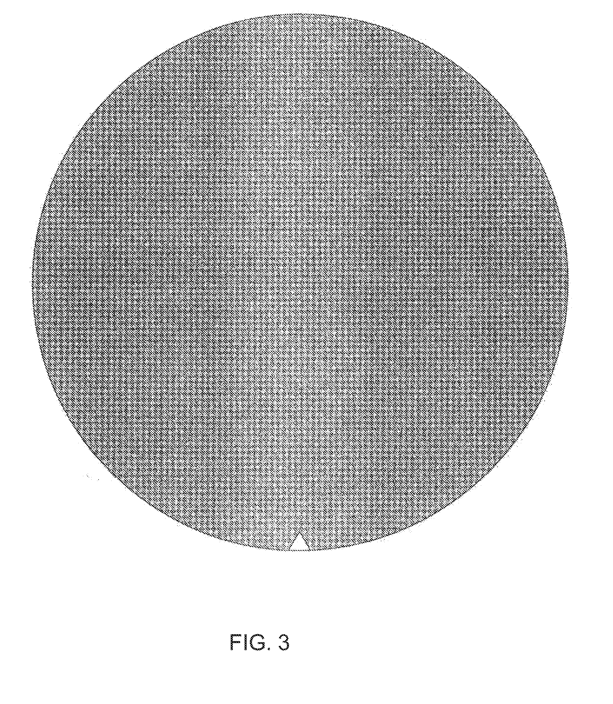
[0115]A laser mark for ID recognition defined under the SEMI specification was formed over the entire mirror surface of an 8-inch silicon wafer to obtain a wafer (3) as shown in FIG. 3. The polyamic acid solution A described in Example 2 was applied onto the mirror surface of the wafer (3) with a spin coater and dried at 120° C. for 10 minutes to obtain a transfer member provided with polyamic acid (3).

[0116]The transfer member with polyamic acid (3) was heat-treated at 300° C. for 2 hours in an atmosphere of nitrogen to form a polyimide coating film with a thickness of 8 μm, and thus, a transfer member with a cleaning function (3) was obtained.

[0117]The average surface roughness Ra of the cleaning layer of the transfer member provided with a cleaning function (3) was 0.34 μm.

[0118]The cleaning layer of the transfer member provided with a cleaning function (3) was peeled from the silicon wafer, and the 180° peeling adhesion (measured in accordance with JIS-Z-0237) with respect to th...


PUM


Abstract

Provided are a cleaning sheet and a transfer member provided with a cleaning function, which are excellent in foreign matter removing performance and transfer performance and which are capable of removing foreign matters each having a predetermined particle diameter particularly efficiently. The cleaning sheet of the present invention includes a cleaning layer substantially free of an adhesive ability, in which: the cleaning layer has an uneven portion having an average surface roughness Ra of 0.10 μm or more; and the cleaning layer has a 180° peeling adhesion of less than 0.20 N / 10 mm, which is defined by JIS-Z-0237 with respect to a mirror surface of a silicon wafer. The transfer member provided with a cleaning function of the present invention includes a transfer member and the cleaning layer of the present invention provided on at least one surface of the transfer member.

Description

TECHNICAL FIELD[0001]The present invention relates to a cleaning sheet and a transfer member provided with a cleaning function. More specifically, the present invention relates to a cleaning sheet and a transfer member provided with a cleaning function, which have excellent foreign matter removal performance and transfer performance and which can remove foreign matter each having a predetermined particle diameter with particularly high efficiency. The present invention also relates to a method of cleaning a substrate processing apparatus using such cleaning sheet and transfer member provided with a cleaning function, and to a substrate processing apparatus cleaned using such cleaning method.BACKGROUND ART[0002]In various kinds of substrate processing apparatuses that are apt to be easily damaged by foreign matter, such as a production apparatus and an inspection apparatus of a semiconductor, a flat panel display, and a printed board, each transfer system and substrate are transferre...

Claims


Application Information

Patent Timeline
Patent Type & Authority Applications(United States)
IPC IPC(8): B08B1/00H01L21/02
CPCB08B1/00C09J7/026B08B7/0028B08B7/00C09J7/22B08B1/143B08B1/10B08B1/30H01L21/304H01L21/00H01L21/02H01L21/0201H01L21/0209H01L21/02041H01L21/02043
Inventor UENDA, DAISUKE
Owner NITTO DENKO CORP
Features
  • R&D
  • Intellectual Property
  • Life Sciences
  • Materials
  • Tech Scout
  • Unparalleled Data Quality
  • Higher Quality Content
  • 60% Fewer Hallucinations
Learn More