Electronic device, electronic apparatus, and electronic device manufacturing method

Active Publication Date: 2012-02-23
SEIKO INSTR INC
View PDF6 Cites 6 Cited by
  • Summary
  • Abstract
  • Description
  • Claims
  • Application Information

AI Technical Summary

Benefits of technology

[0028]The electronic device manufacturing method may further include a step of dividing a plurality of electronic devices into individual electronic devices after forming the plurality of electronic devices on the single base in a bundle. According to this configuration, it is possible to manufacture electronic devices according to an aspect of the invention in a bundle, thereby reducing the manufacturing time, the number of process steps, and the cost in the mas

Problems solved by technology

However, since this package is formed of a glass-ceramic composite, the package is manufactured by individual production of placing a quartz crystal chip on a base and covering the

Method used


Image

  • Electronic device, electronic apparatus, and electronic device manufacturing method
  • Electronic device, electronic apparatus, and electronic device manufacturing method
  • Electronic device, electronic apparatus, and electronic device manufacturing method

Examples


Example

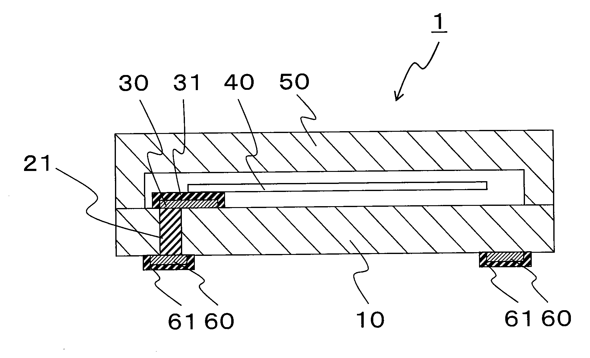
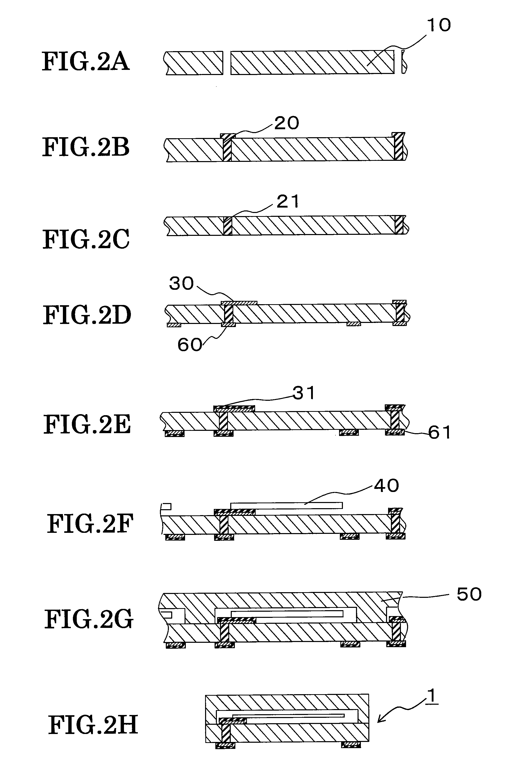
[0043]Hereinafter, an embodiment of the invention will be described in detail with reference to the accompanying drawings. FIG. 1 is a sectional view illustrating an electronic device according to an embodiment of the invention. In the electronic device 1, an electronic component 40 is mounted into a cavity section isolated from external air and surrounded with a base 10 and a cap 50 formed of glass. The electronic component 40 is electrically connected to an external electrode 61, which is a terminal mounted on a substrate, via an internal wiring 31, a circuit pattern 30, a through-electrode 21, and an electrode pattern 60. The cap 50 is not limited to glass, but may be formed of, for example, silicon, which can be used for an MEMS device such as a pressure sensor. The cap 50 may be formed of aluminum.

[0044]The electronic device 1 shown in FIG. 1 is a crystal oscillator in which a tuning-fork crystal oscillator chip is mounted as the electronic component 40. In the embodiment of th...


PUM


Abstract

An electronic device is provided which includes a base, a through-electrode that passes through the base and from which an insulating material on an end face thereof is removed by polishing, a circuit pattern that is formed on an end face of the through-electrode, an electronic component that is disposed via an internal wiring formed on the circuit pattern, an electrode pattern that is formed on the surface of the base opposite to the surface on which the electronic component is disposed and that is connected to the other end face of the through-electrode, an external electrode that is formed on the electrode pattern, and a cap that is bonded to the base so as to protect the electronic component on the base.

Description

RELATED APPLICATIONS[0001]This application claims priority under 35 U.S.C. §119 to Japanese Patent Application No. 2010-186312 filed on Aug. 23, 2010, the entire content of which is hereby incorporated by reference.BACKGROUND OF THE INVENTION[0002]1. Field of the Invention[0003]The present invention relates to an electronic device such as a crystal oscillator chip or a piezoelectric device and a manufacturing method thereof.[0004]2. Description of the Related Art[0005]Since a crystal oscillator has an excellent frequency characteristic, the crystal oscillator is widely used as a component to be mounted on a printed circuit board. However, in order to stabilize the characteristics of the crystal oscillator, the crystal oscillator is preferably received in a hermetic container to block the influence of external air. “GLASS-CERAMIC COMPOSITE AND FLAT PACKAGE TYPE PIEZOELECTRIC COMPONENT USING THE SAME” (JP-A-11-302034) is proposed as an example of such a package structure.[0006]This pa...

Claims


Application Information

Patent Timeline
IPC IPC(8): H03B5/30H05K3/00
CPCB81B7/007Y10T29/49124H03H9/1021H01L2224/81895H01L2924/161H01L23/10H01L21/486H01L21/50H01L24/13H01L24/16H01L24/29H01L24/32H01L24/81H01L24/83H05K1/114H05K3/4046H01L2224/13144H01L2224/16227H01L2224/29339H01L2224/32227H01L2224/81191H01L2224/81203H01L2224/81444H01L2224/832H01L2224/83801H05K2201/10075H05K2201/10371H01L2224/29294B81B2207/096H01L2924/1461H01L2224/16225H01L23/49827H01L2924/00014H01L2924/00
Inventor NAKAMURA, TAKAHIKOSATO, KEIJITAKEUCHI, HITOSHIARATAKE, KIYOSHINUMATA, MASASHI
Owner SEIKO INSTR INC
Why Eureka
Try Eureka