Cu-ga alloy sputtering target and manufacturing method thereof

a technology of sputtering target and ge alloy, which is applied in the direction of metallic material coating process, diaphragm, inorganic chemistry, etc., can solve the problems of increasing size, microscopic uniformity of material components, and relatively slow cooling of casting after casting, so as to reduce the probability of arcing or cracking, good yield, and reduce the effect of porosity

Inactive Publication Date: 2012-02-23
KOBELCO RES INST
View PDF6 Cites 22 Cited by
  • Summary
  • Abstract
  • Description
  • Claims
  • Application Information

AI Technical Summary

Benefits of technology

[0023]In accordance with the present invention, it is possible to implement a Cu—Ga alloy sputtering target in which the crystal grains are refined, and the porosity is reduced, and which preferably has a morphology of a specific compound phase. As a result, when sputtering is performed using the target, arcing occurrence or cracking is suppressed. Accordingly, it is possible to form a Cu—Ga sputtering film having a uniform film composition with stability and efficiency, and further with a good yield as, for example, a layer forming an optical absorption layer of a CIS (CIGS) type thin film solar cell.

Problems solved by technology

However, manufacturing with the method results in that cooling after casting relatively slowly proceeds.
Accordingly, the crystal structure increases in size, so that microscopic ununiformity of the material component occurs.
This conceivably contributes to the reduction of the conversion efficiency of the solar cell.
Further, in the sputtering target manufactured with a melting / casting method, pores (voids) tend to be formed.
Accordingly, the discharge stability of sputtering is deteriorated, and the shock of arcing generates particles, which are deposited on a substrate.
This and other factors reduce the adhesion between the film and the substrate, which unfavorably results in the deterioration of the performances of the solar cell.
Further, the sputtering target manufactured by a melting / casting method has a low strength.
For this reason, the target unfavorably tends to be broken due to the stress caused by the increase in temperature of the target during sputtering.
However, there is a limit on the refinement of the power prior to sintering, and resultingly, there is a limit on the refinement of the crystal structure.
Further, there is also a limit on uniform mixing of powders.

Method used


Image

  • Cu-ga alloy sputtering target and manufacturing method thereof
  • Cu-ga alloy sputtering target and manufacturing method thereof
  • Cu-ga alloy sputtering target and manufacturing method thereof

Examples


examples

[0054]Below, the present invention will be described more specifically by way of examples. However, the present invention is by no means limited by the following examples, and can naturally be put into practice by adding appropriate changes within the scope applicable to the gists described above and later. All of these are included in the technical scope of the present invention

examples 1 and 2

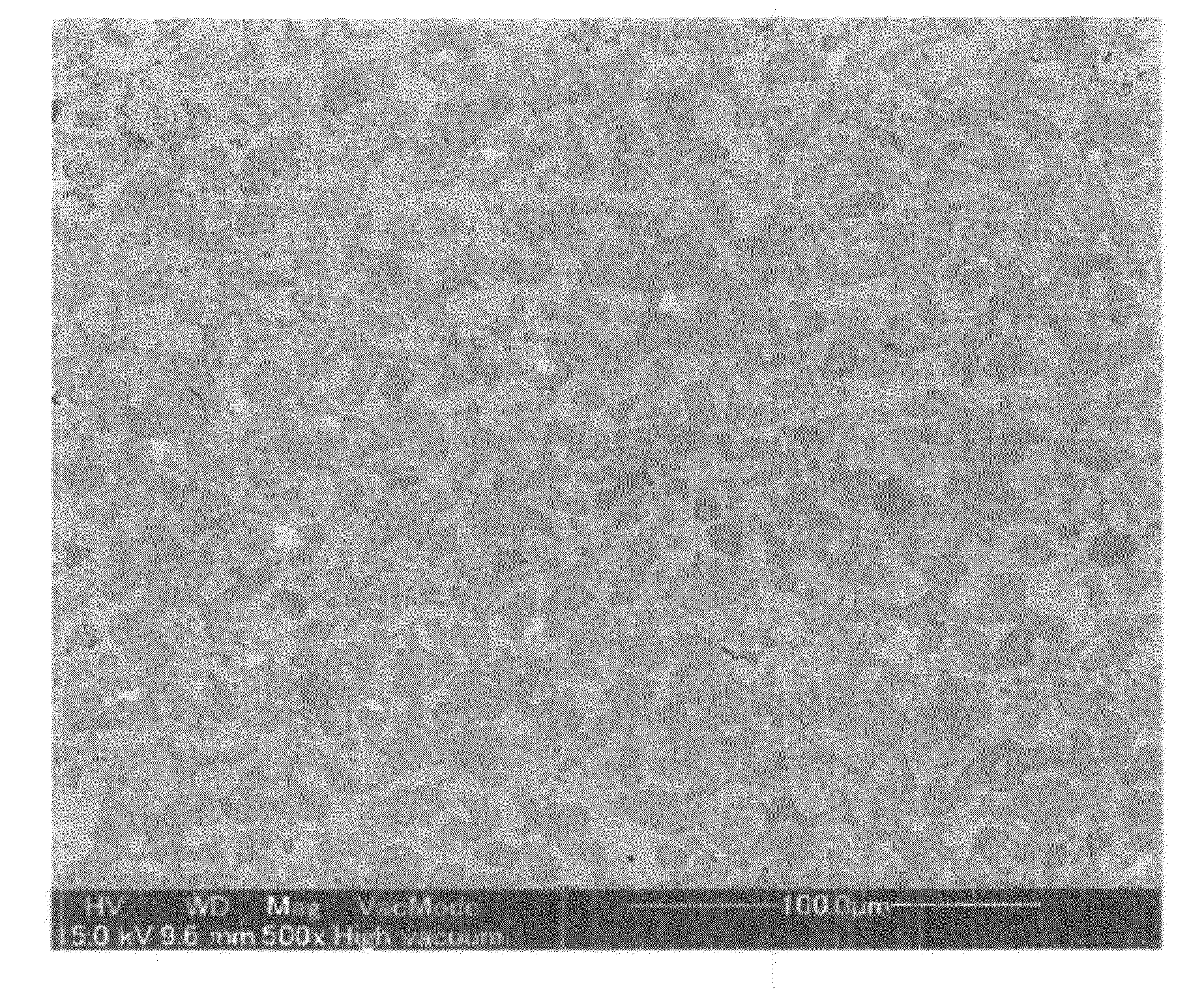
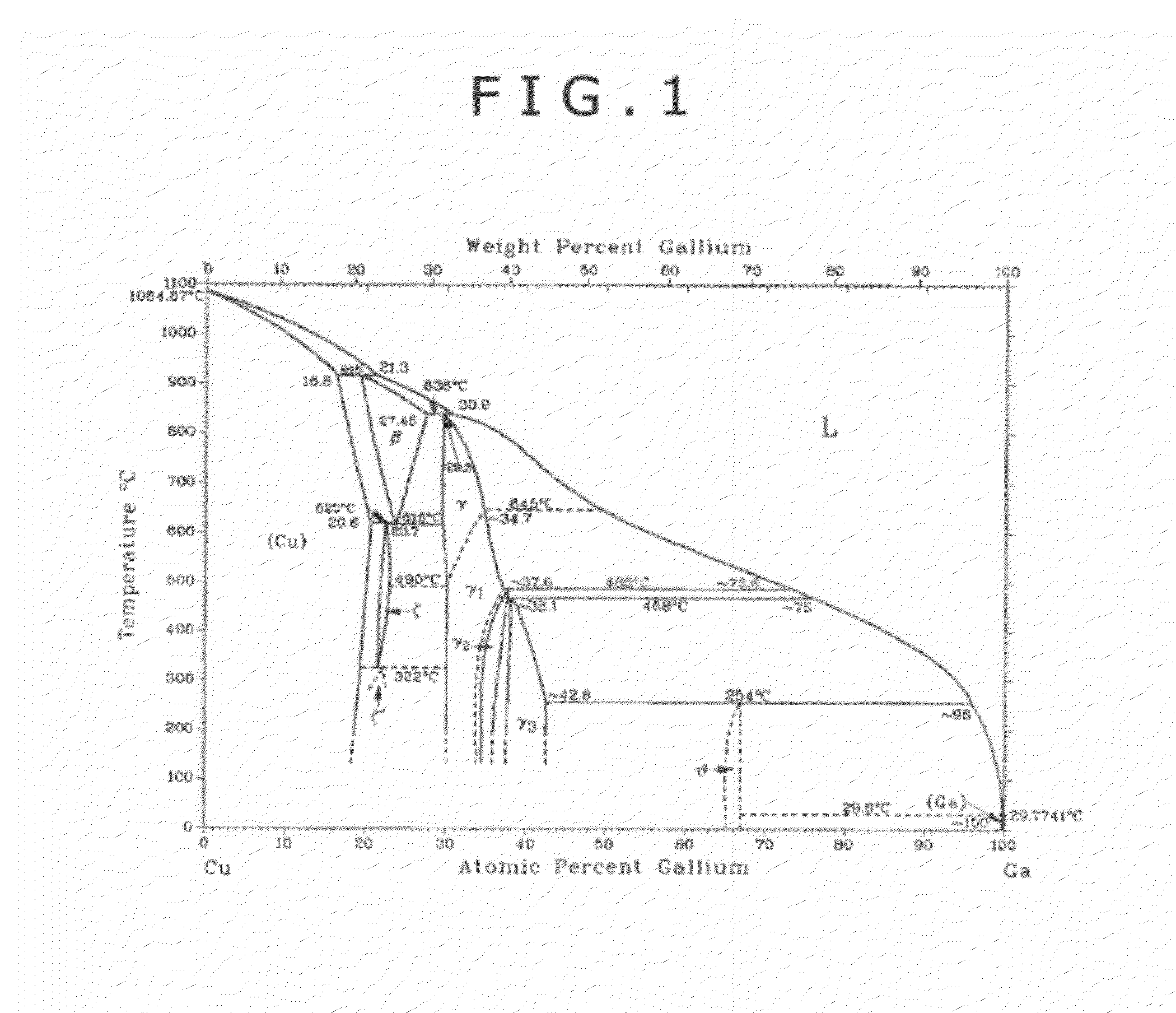
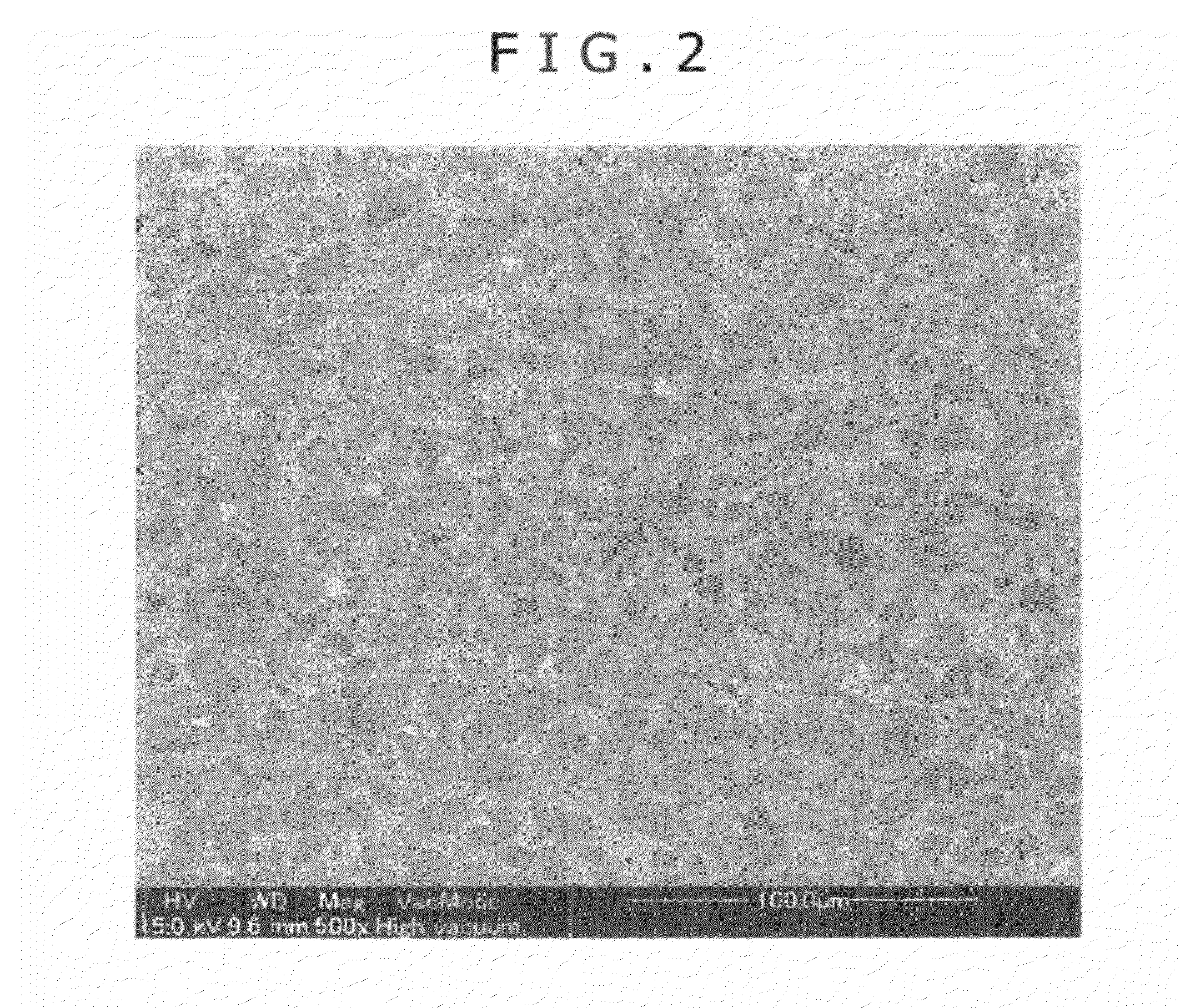
[0055]A molten metal of a Cu—Ga alloy containing Ga in an amount of 25 at %, and including the balance of Cu and inevitable impurities was obtained from heating to 1200° C. in an induction melting furnace. Then, the molten metal was flowed from a nozzle set at the lower part of the induction melting furnace. A nitrogen gas was sprayed to the flowed molten metal, resulting in fine droplets. The droplets were uniformly piled up on a collector at a tilt angle of 35°, rotating at a distance (spray distance) of 500 to 1000 mm from the nozzle in a gas metal ratio of 2.0 to 8.0 Nm3 / kg. As a result, a Cu—Ga alloy preform (density: about 75 vol %) was manufactured. The Cu—Ga alloy preform manufactured by the spray forming method was sealed and subjected to hot isostatic pressing (HIP) under a temperature of 500° C. to 600° C. and under a pressure of 80 MPa or more, resulting in a Cu—Ga densified product.

[0056]Then, the resulting densified product was machined to manufacture a Cu—Ga alloy spu...


PUM

PropertyMeasurementUnit
porosityaaaaaaaaaa
grain sizeaaaaaaaaaa
lengthaaaaaaaaaa

Abstract

Disclosed is a Cu—Ga alloy sputtering target which enables the formation of a Cu—Ga sputtering film having excellent uniformity in film component composition (film uniformity), enables the reduction of occurrence of arcing during sputtering, has high strength, and rarely undergoes cracking during sputtering. Specifically disclosed is a Cu—Ga alloy sputtering target which comprises a Cu-based alloy containing Ga, has an average crystal particle diameter of 10 μm or less, and has a porosity of 0.1% or less.

Description

TECHNICAL FIELD[0001]The present invention relates to a Cu—Ge alloy sputtering target and a manufacturing method thereof. It relates to a Cu—Ga alloy sputtering target for use in, for example, the formation of an optical absorption layer of a CIS (CIGS) type thin film solar cell, and a manufacturing method thereof.BACKGROUND ART[0002]As the formation method of the optical absorption layer of the CIS (CIGS) type thin film solar cell, a Cu—Ga alloy layer and an In layer are sequentially formed to be stacked by a sputtering method (e.g., see Patent Document 1). Further, as the sputtering target for use in the formation of the Cu—Ga alloy layer, there is generally used, for example, the one with a Ga content of 10 to 30 at %.[0003]As the manufacturing method of the sputtering target, mention may be made of manufacturing with a melting / casting method as shown in, for example, Patent Document 2. However, manufacturing with the method results in that cooling after casting relatively slowly...

Claims


Application Information

Patent Timeline
Patent Type & Authority Applications(United States)
IPC IPC(8): B32B15/00B05D3/02B05D3/00C23C14/14C23C14/34
CPCB22F2998/10C22C1/0425C23C14/3414C22C9/00B22F9/082C23C14/34B22F3/15B22F3/12B22F9/08
Inventor MATSUMURA, HIROMINANBU, AKIRAEHIRA, MASAYAOKAMOTO, SHINYA
Owner KOBELCO RES INST
Why Eureka
Try Eureka