
Method for fabricating an integrated-passives device with a MIM capacitor and a high-accuracy resistor on top

a technology of integrated passives and resistors, which is applied in the direction of capacitors, semiconductor devices, electrical devices, etc., can solve the problems of poor top lead of the remaining first cover layer, negatively affecting the structure and reliability of the resistor layer, etc., and achieves high reliability, high accuracy of electrical resistance, and improved fabrication efficiency

Active Publication Date: 2012-02-23
NEXPERIA BV
View PDF5 Cites 6 Cited by
  • Summary
  • Abstract
  • Description
  • Claims
  • Application Information

AI Technical Summary

Benefits of technology

[0013]With the method of the present invention the fabrication of a highly reliable resistor layer on top of an integrated MIM capacitor on a substrate is achieved, that means, the resistor layer can be fabricated to precisely assume a desired electrical resistance. By employing the method of the present invention, the electrical-resistance value of the resistor layer on top of the MIM capacitor is not any more influenced in an uncontrollable manner, as has been observed when employing prior-art fabrication methods. The improved reliability achieved with the method of the present invention is to be understood in the sense that it allows achieving a high accuracy of the electrical resistance for a large number of electronic components fabricated concurrently on a single wafer, and in different processing runs, thus improving the fabrication efficiency and lowering the overall processing cost of the electronic component.
[0014]The method of the invention is based on the recognition that the lead-containing first cover layer is effectively prevented from developing deteriorating effects on the subsequent fabrication of the second cover layer exerted by Pb particles on the surface of the first cover layer formed during the deposition of the second cover layer. Such Pb particles have been found to originate from reduced oxidized Pb species from the lead-containing first cover layer. By thinning the first cover layer, most of the disturbing Pb particles are removed from the top surface of the lead-containing first cover layer. The thinning of the first cover layer leads to a more than proportional removal of the lead. Due to this effect the top of the remaining first cover layer is lead poor. This suppresses a catalytic growth mechanism of nanostructures during the initial growth stages of the fabrication of the second cover layer, which would result in a strong surface roughness of the second cover layer, which intern would negatively affect the structure and reliability of the resistor layer.
[0017]While the application of the method of the present invention is not restricted to the field of fabricating electronic components with high-K MIM capacitors, they do form a preferred field of application. High-K MIM capacitors are very advantageous for operation under voltages even higher than 10 V. The method of the invention allows improving the advantageous combination of such high-K MIM capacitors with resistors in a stacked arrangement. The term high-K capacitor as used herein refers to capacitors with a high-K capacitor dielectric between the top and bottom electrodes. Such high-K MIM capacitor dielectrics may for instance have a relative dielectric permittivity of between 100 and 5000. Such high values of the relative dielectric permittivity are for instance achieved by magnesium-doped lead niobate, lead titanate, i.e., PMNPT, or lead zirconate titanate i.e., PZT, which may or may not be doped. MIM capacitors based on such high-K materials can be used to obtain capacitance densities up to 100 nF / mm2.
[0019]For embodiments having a lead-containing capacitor dielectric, the lead-containing first cover layer provides a particular advantage in that the capacitor dielectric achieves a very high dielectric constant, which would in absence of the lead-containing first cover layer be negatively affected and thus be much lower. Using for instance lead-containing perovskite dielectrics, like PZT for both the capacitor dielectric and for the first cover layer allows achieving a capacitor dielectric with a dielectric constant of up to 1700. Also, the breakdown voltage of the MIM capacitor can be made particularly high, depending, of course, on the thickness of the capacitor dielectric. The lead-containing first cover layer achieves this advantage of a high dielectric constant and a high breakdown voltage also for other lead-containing dielectric materials, such as PLZT or PNMPT.
[0022]The thinning is preferably performed to remove between 10 and 50 nm of the first cover layer. Removing this surface section of the first cover layer effectively avoids the creation of Pb particles originating from reduction processes of lead oxide, which is reduced to Pb particles during the deposition of the second cover layer. Thinning leads to a lead-poor surface of the first cover layer. In other words, the thinning will predominantly remove such Pb particles from the surface of the first cover layer.
[0030]The electronic component of the present invention or any of its embodiments disclosed herein is advantageously integrated with at least one active semiconductor element like a diode or a transistor, formed in the same substrate. This way, an electronic device with integrated active and passive circuit elements on the same substrate is fabricated. A particularly high integration density can be obtained for such an electronic device, since the electronic component has the resistors arranged on top of the MIM capacitors, thus allowing considerable savings of chip area.

Problems solved by technology

Due to this effect the top of the remaining first cover layer is lead poor.
This suppresses a catalytic growth mechanism of nanostructures during the initial growth stages of the fabrication of the second cover layer, which would result in a strong surface roughness of the second cover layer, which intern would negatively affect the structure and reliability of the resistor layer.

Method used


Image

  • Method for fabricating an integrated-passives device with a MIM capacitor and a high-accuracy resistor on top
  • Method for fabricating an integrated-passives device with a MIM capacitor and a high-accuracy resistor on top
  • Method for fabricating an integrated-passives device with a MIM capacitor and a high-accuracy resistor on top

Examples


Embodiment Construction

[0033]The present invention is further elucidated by the following figures and examples, which are not intended to limit the scope of the invention. The person skilled in the art will understand that various embodiments may be combined.

BRIEF DESCRIPTION OF THE DRAWINGS

[0034]These and other aspects of the invention will be apparent from and elucidated with reference to the embodiment(s) described hereinafter. In the following drawings.

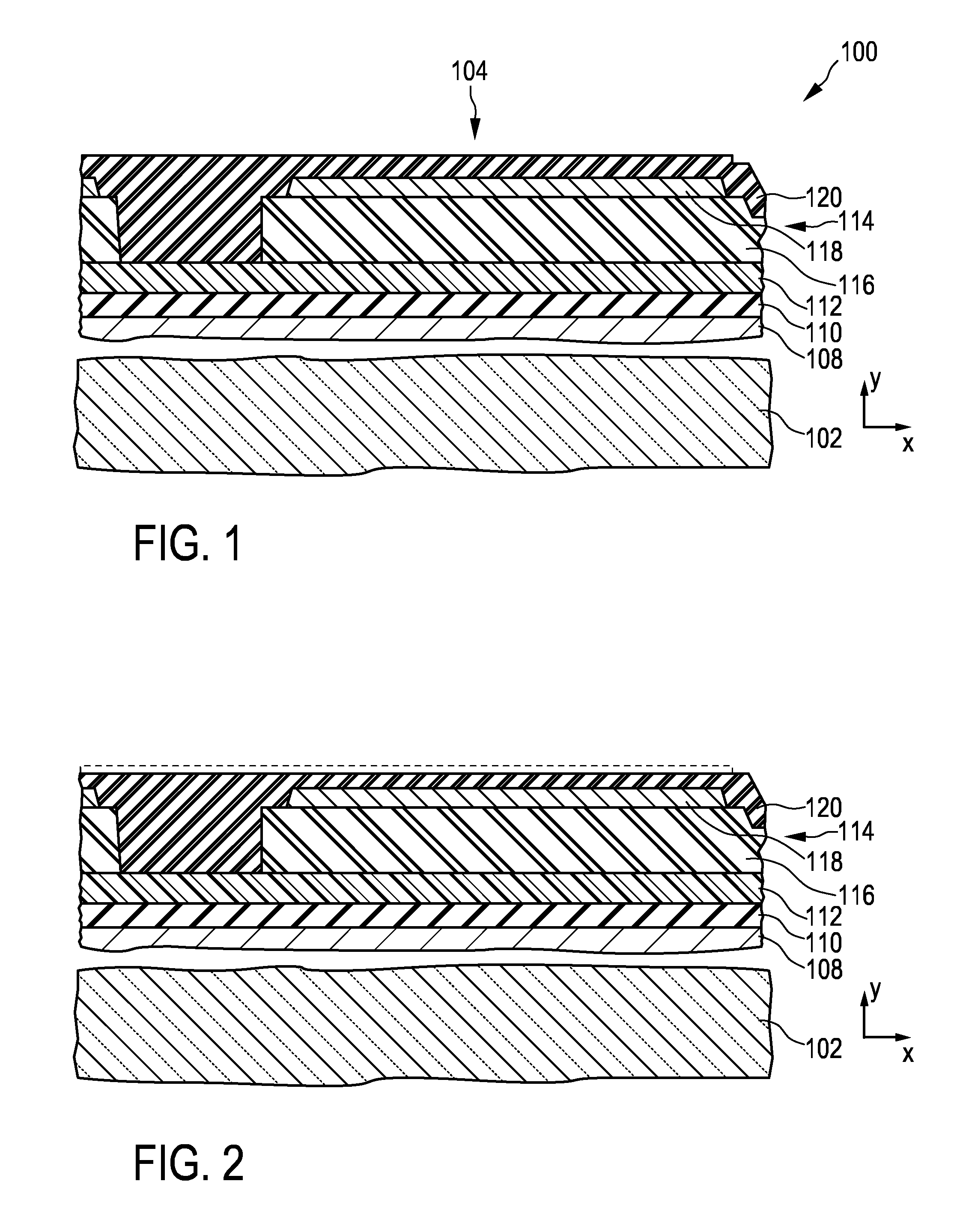
[0035]FIG. 1 shows a schematic cross-sectional view of an electronic component at a first processing stage of a method according to the present invention;

[0036]FIG. 2 shows the electronic component of FIG. 1 at a second processing stage;

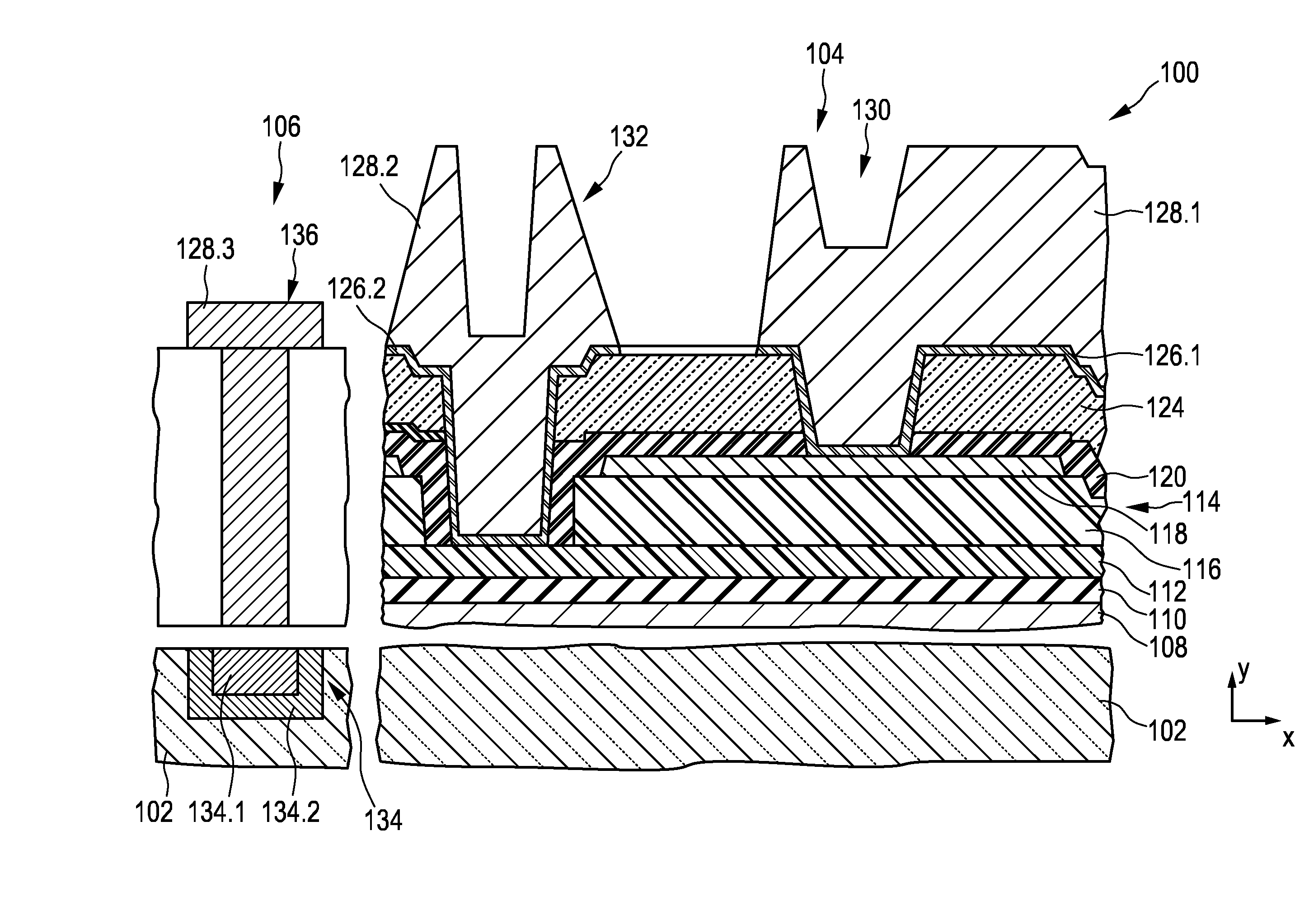
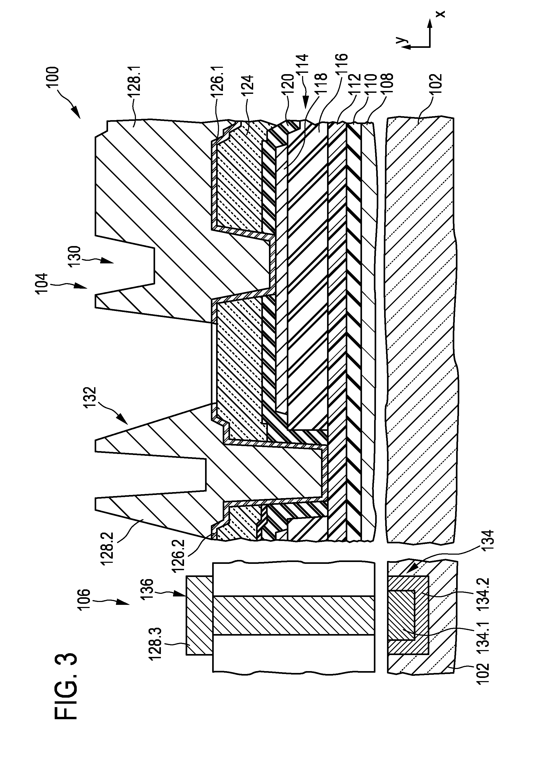
[0037]FIG. 3 shows the electronic component of FIGS. 1 and 2 at a third processing stage, integrated into an electronic device.

DETAILED DESCRIPTION OF THE DRAWINGS

[0038]FIG. 1 shows a schematic cross-sectional view of an electronic component 104 on a substrate 102. Only selected portions of the electronic component are s...


PUM


Abstract

The present invention relates to a method for fabricating an electronic component, comprising fabricating, on a substrate (102) at least one integrated MIM capacitor (114) having a top capacitor electrode (118) and a bottom capacitor electrode (112) at a smaller distance from the substrate than the top capacitor electrode; fabricating an electrically insulating first cover layer (120) on the top capacitor electrode, which first cover layer partly or fully covers the top capacitor electrode and is made of a lead-containing dielectric material; thinning the first cover layer; fabricating an electrically insulating second cover layer (124) on the first cover layer, which second cover layer partly or fully covers the first cover layer and has a dielectric permittivity smaller than that of the first cover layer; and fabricating an electrically conductive resistor layer (126) on the second cover layer, which resistor layer has a defined ohmic resistance.

Description

FIELD OF THE INVENTION[0001]The present invention relates to a method for fabricating an electronic component and for fabricating an electronic device.BACKGROUND OF THE INVENTION[0002]MIM (metal-insulator-metal) capacitors based on high-K dielectrics play an important role for next generation Integrated Discretes (IDs) devices. Such Integrated Discretes devices comprise for instance capacitors, resistors and ESD protection diodes.[0003]US 2008 / 0001292 A1 describes an electronic component with an integrated thin-film MIM capacitor structure on a substrate. The thin-film capacitor includes a pyrochlore or perovskite alkali earth dielectric layer between a plurality of electrode layers. A pyrochlore or perovskite hydrogen-gettering cover layer is deposited over the thin-film capacitor. It is in different embodiments made of (Bax Sry)TiO3 (BST), BaTi03, CaTi03, SrTi03, BeTi03, MbTi03 or a mix of these materials. The hydrogen-gettering cover layer prevents hydrogen from reacting with and...

Claims


Application Information

Patent Timeline
Patent Type & Authority Applications(United States)
IPC IPC(8): H01L21/02
CPCH01L27/016H01L27/0251H01L28/65H01L28/20H01L28/55H01L27/0688
Inventor ROEST, AARNOUD LAURENSVAN LEUKEN-PETERS, LINDA
Owner NEXPERIA BV
Learn More