

Semiconductor light-emitting element, method for producing the same, lamp, lighting device, electronic equipment, mechanical device and electrode
Image

Examples
first embodiment
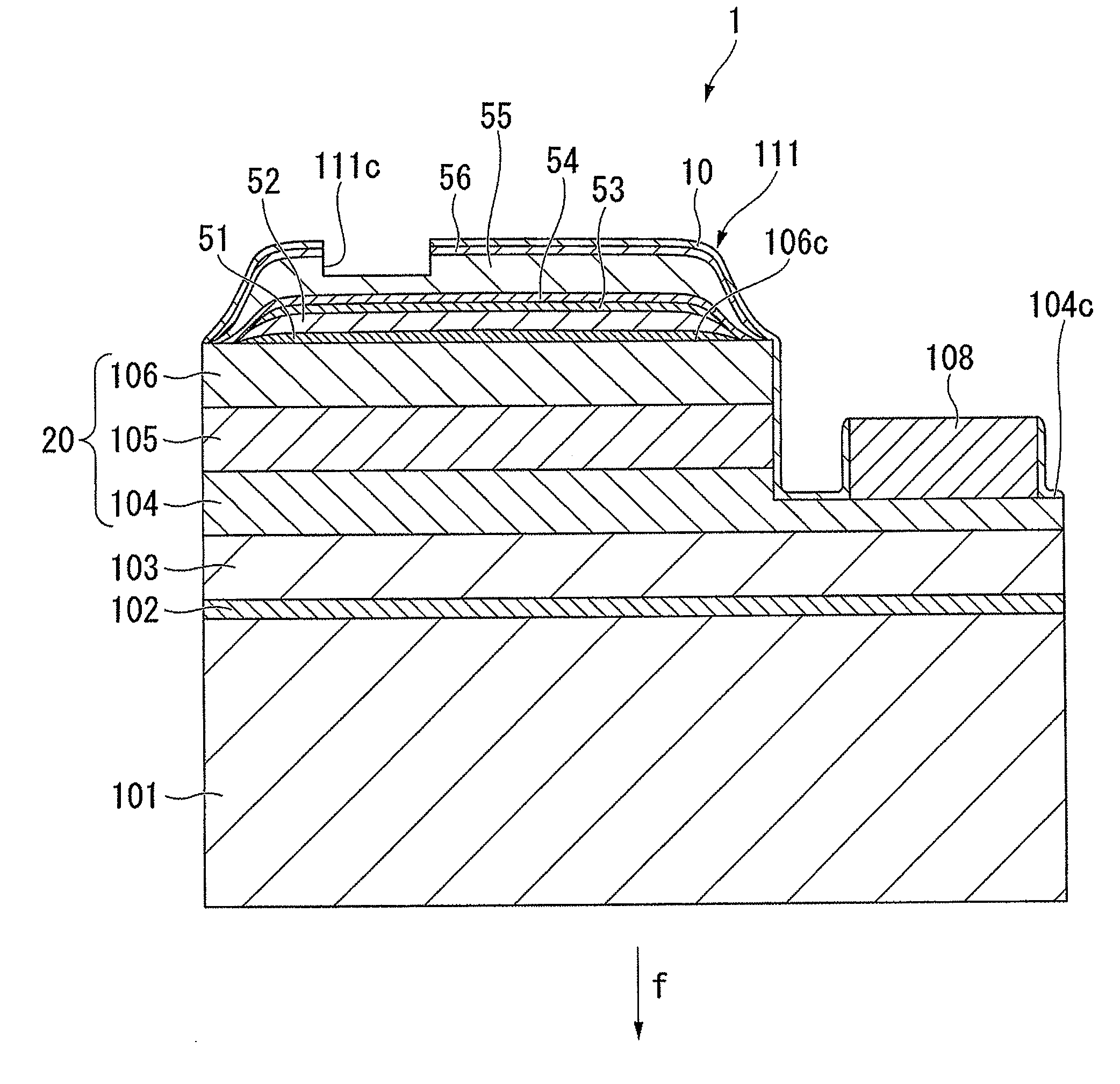
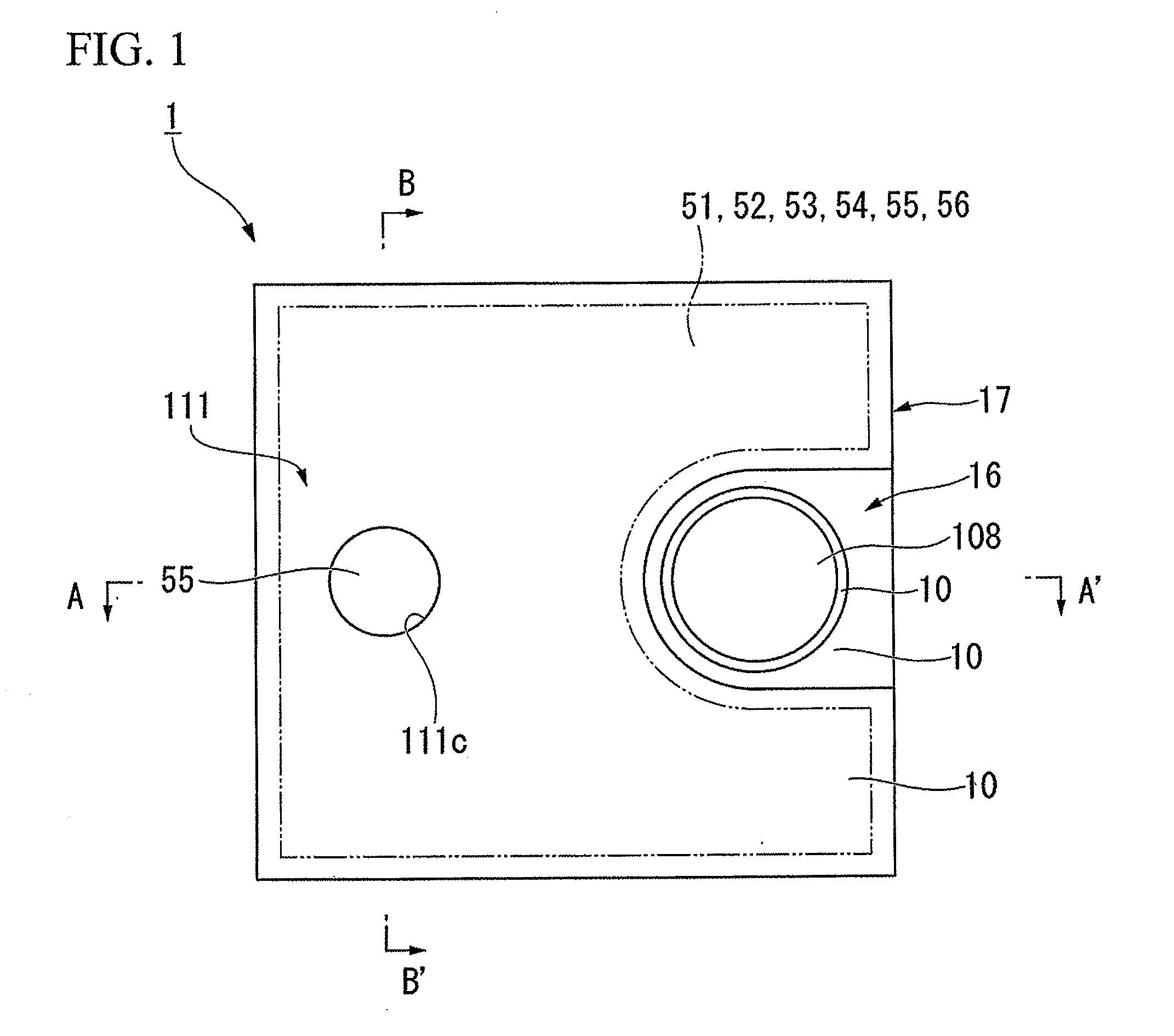
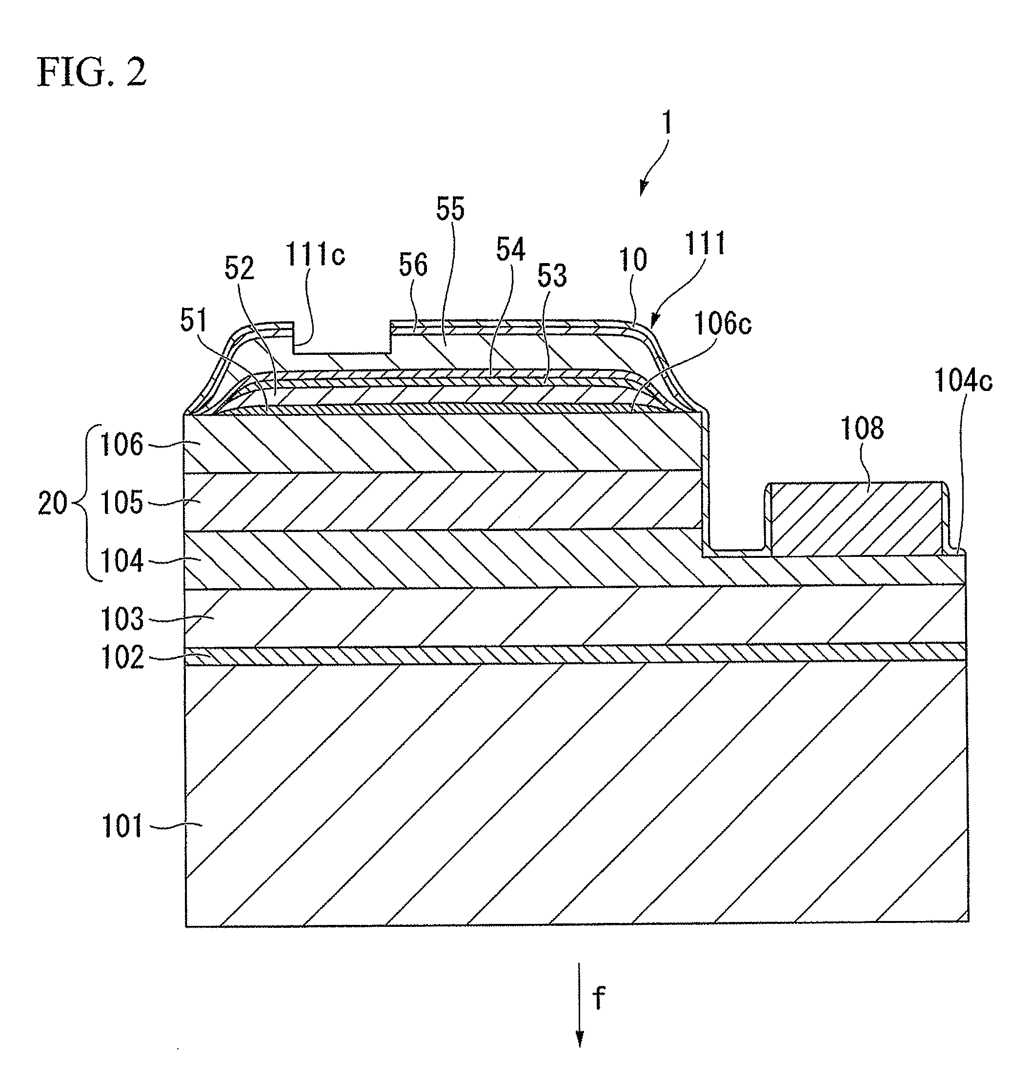
[0089]FIGS. 1 to 5 show an example of a semiconductor light-emitting element, which is an embodiment of the present invention. FIG. 1 is a schematic plan view of the semiconductor light-emitting element, which is the embodiment of the present invention, FIG. 2 is a schematic cross-sectional view taken along lines A-A′ in FIG. 1, FIG. 3 is a schematic cross-sectional view taken along lines B-B′ in FIG. 1, FIG. 4 is a schematic cross-sectional view of a laminated semiconductor layer which constitutes the semiconductor light-emitting element shown in FIG. 1, and FIG. 5 is an enlarged cross-sectional view of a p-type electrode of the semiconductor light-emitting element shown in FIG. 1.
(Semiconductor Light Emitting Element)
[0090]As shown in FIG. 1, a semiconductor light-emitting element 1 has a rectangular shape in a plan view. One side thereof is cut away in a half-circular and half-rectangular shape, so that a cutout 16 and a cutout body 17 are defined.
[0091]An n-type electrode 108 ha...
second embodiment
[0266]FIG. 10 is a schematic cross-sectional view showing an example of a lamp, which is an embodiment of the present invention. In the figures referred to in the following description, size, thickness, dimensions and the like of the members shown in the figures do not correspond to the actual dimensions of the semiconductor light-emitting element and the like.
[0267]As shown in FIG. 10, a lamp 4 of the embodiment of the present invention is a chip for board mounting, and the semiconductor light-emitting element 1 described in the first embodiment is used therein.
[0268]The lamp 4 is, for example, a combination of the semiconductor light-emitting element 1 and a phosphor, and may have any constitution known in the art and may be produced by means known in the art. It is known that emission color can be changed by the combination of the semiconductor light-emitting element 1 and phosphor, and it is not limited at all to employ such techniques in the embodiment lamp of the present inven...
example 1
Preparation of Semiconductor Light Emitting Element
[0281]A semiconductor light-emitting element of gallium nitride-based compound semiconductor described in the first embodiment was produced as follows.
[0282]First, a base layer of undoped GaN having 8 μm thickness was formed onto a sapphire substrate via a buffer layer of AlN.
[0283]Next, after an Si doped n-type GaN contact layer having 2 μm thickness and an n-type In0.1Ga0.9N clad layer having 250 nm thickness was formed, Si doped GaN barrier layers of 16 nm thickness and In0.2Ga0.8N well layers of 2.5 nm thickness were laminated alternately respectively for 5 times and further finished with the barrier layer, so that a light-emitting layer having a multiple quantum well structure was formed.
[0284]Further, an Mg doped p-type Al0.07Ga0.93N clad layer having a thickness of 10 nm and an Mg doped p-type GaN contact layer having a thickness of 150 nm were sequentially formed.
[0285]These gallium nitride-based compound semiconductor layer...
PUM
 Abstract
Description
Claims
Application Information
- IPC
- H01L33/60
- CPC
- H01L33/38; H01L2224/13; H01L2933/0016; H01L33/405
- Inventors
- OKABE, TAKEHIKO; MASUYA, KYOSUKE