Method of fabricating soi super-junction ldmos structure capable of completely eliminating substrate-assisted depletion effects
- Summary
- Abstract
- Description
- Claims
- Application Information
AI Technical Summary
Benefits of technology
Problems solved by technology
Method used
Image
Examples
embodiment 1
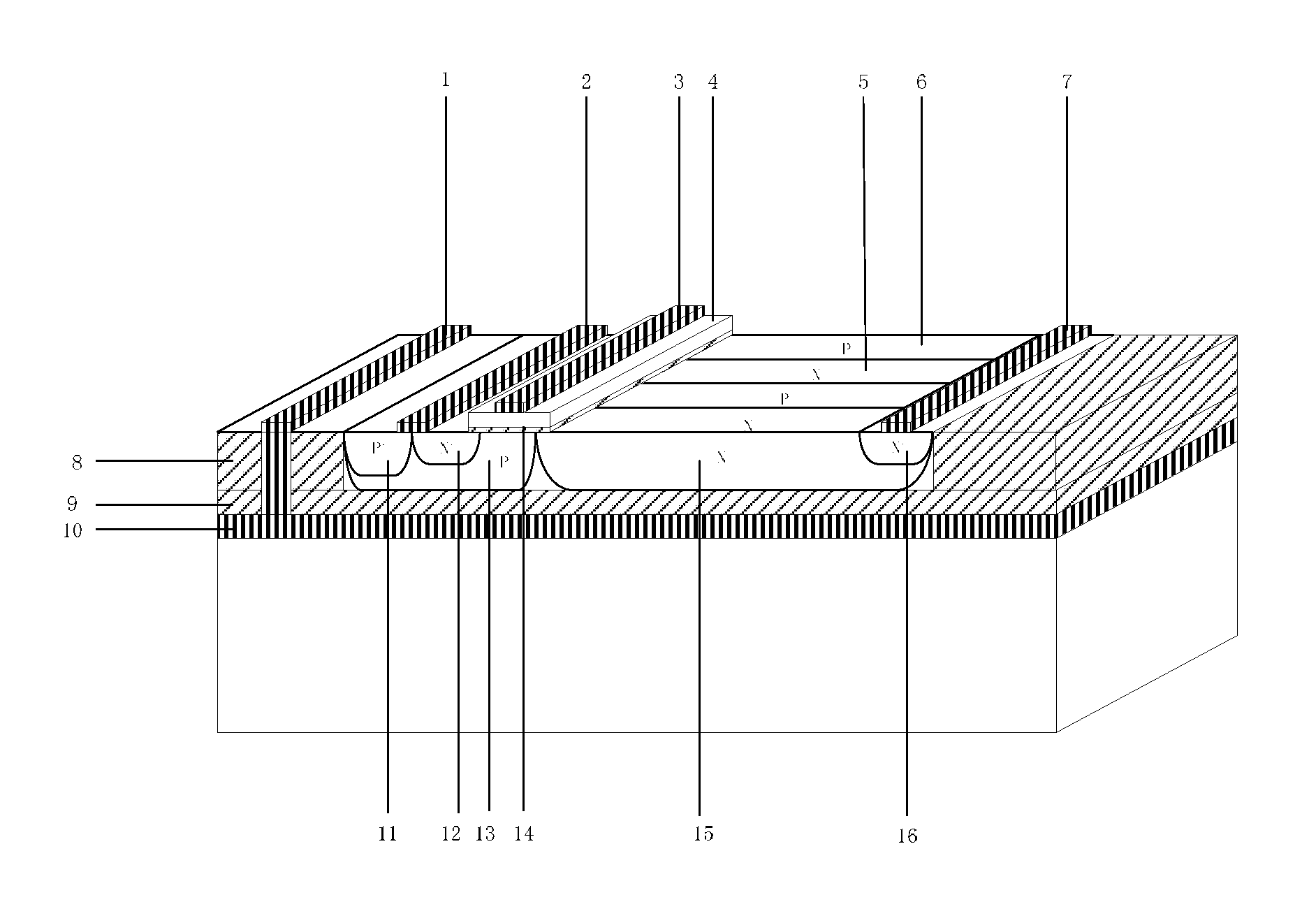
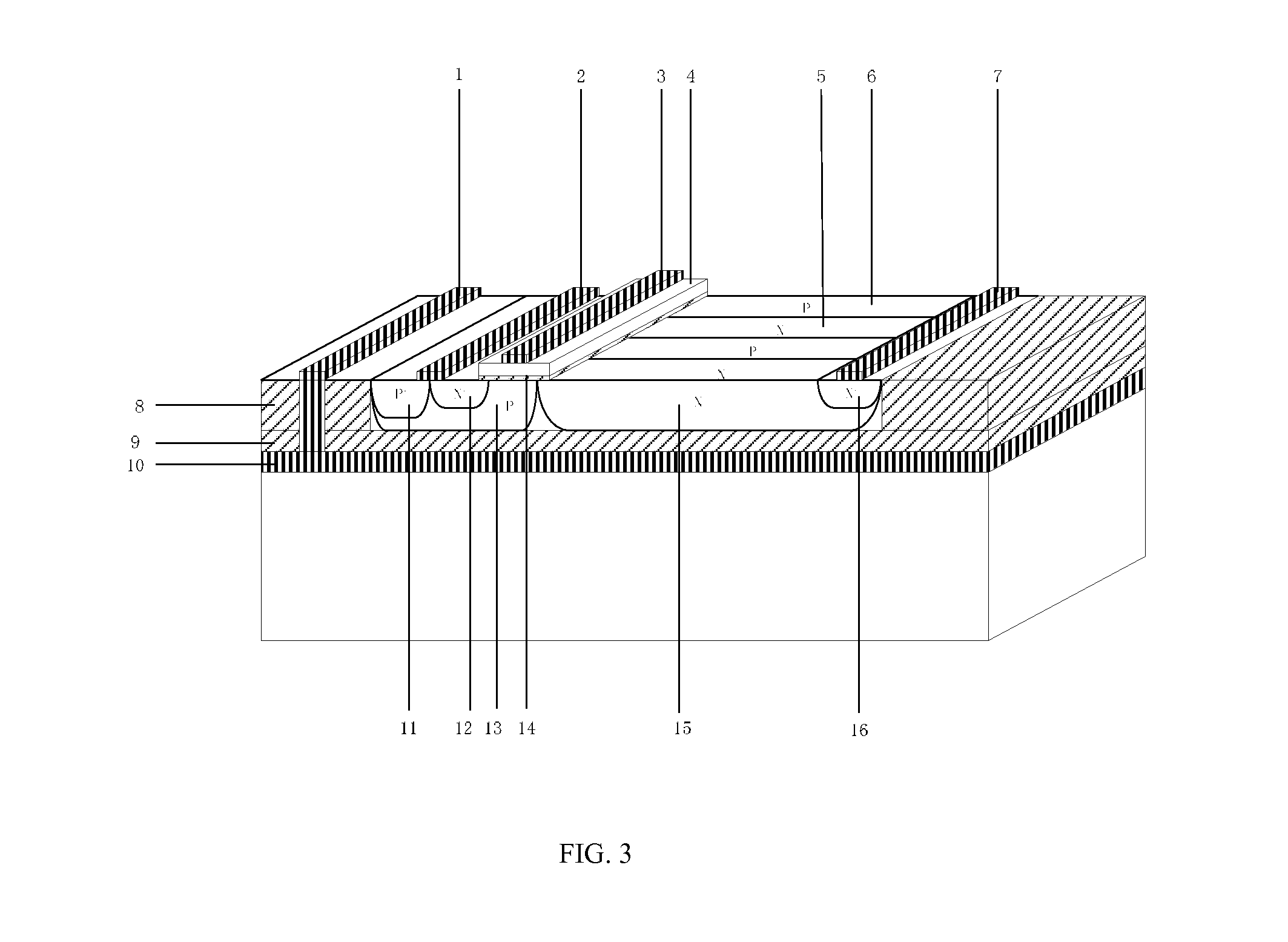
[0038]This embodiment provides a silicon-on-insulator super-junction lateral double-diffused MOSFET (abbreviated as SOI SJ LDMOS) structure. As shown in FIGS. 1 to 3, the structure includes a silicon film, a conductive layer 10, a buried oxide layer 9, an active region, a trench isolation structure 8 and an electrode. The silicon film is located at the bottom of the SOI SJ LDMOS structure. The conductive layer 10 including a charge conducting layer and a barrier layer is located on an upper surface of the silicon film, wherein the barrier layer is grown on both an upper surface and a lower surface of the charge conducting layer. The buried oxide layer 9 is located on an upper surface of the conductive layer 10, and the active region includes a source region 12, a trench region 13, a drain region 16, a drift region 15, a gate region 4 which is located on an upper surface of the trench region 13, and a gate oxide layer 14 which is located between the gate region 4 and the trench regio...
embodiment 2
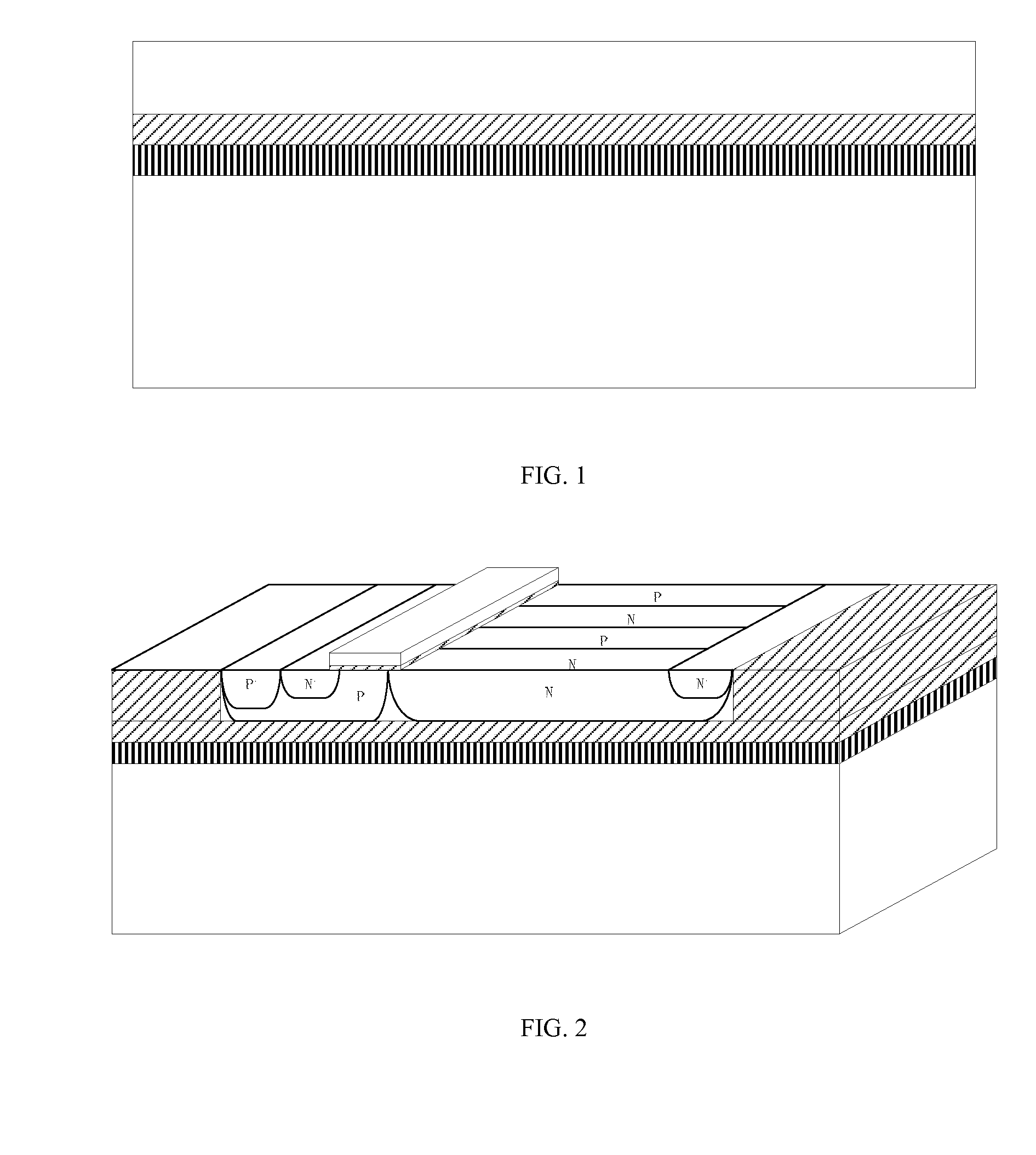
[0040]This embodiment provides a method of fabricating a SOI super-junction LDMOS structure capable of completely eliminating the substrate-assisted depletion effects, and the method includes the following steps.[0041](1) Firstly, a conductive layer is prepared below a buried oxygen layer of a SOI structure using the bonding technique by:
[0042]a) depositing a tantalum nitride barrier layer (about 75 angstroms) on a first bulk silicon wafer, and then depositing a copper layer which is half as thick as a metallic conduction layer to be grown;
[0043]b) forming a silicon dioxide layer on a second bulk silicon wafer by thermal oxidation, and then depositing a tantalum nitride barrier layer (about 75 angstroms) and a copper layer which is half as thick as the metallic conduction layer to be grown;
[0044]c) bonding the first bulk silicon wafer and the second bulk silicon wafer using the metallic bonding technique; and
[0045]d) decreasing a size of the second bulk silicon wafer at its back usi...
PUM
 Abstract
Description
Claims
Application Information


