High- frequency power amplifier

Active Publication Date: 2012-04-26
PANASONIC SEMICON SOLUTIONS CO LTD
View PDF5 Cites 14 Cited by
  • Summary
  • Abstract
  • Description
  • Claims
  • Application Information

AI Technical Summary

Benefits of technology

[0022]In accordance with the present invention, the power consumed inside the amplifying element can be reduced because the distortion of the drain voltage waveform and drain current waveform ca

Problems solved by technology

However, radio frequency power amplifiers require a large amount of power and consume most of the supplied power needed to drive radio frequency generator circuits or transmitter circuits, hindering the low power consumption of mobile communication terminals and base stations.
Compared to operation in a linear region, operation in a saturation region produces high power added efficiency, but signal distortion is also generate

Method used


Image

  • High- frequency power amplifier
  • High- frequency power amplifier
  • High- frequency power amplifier

Examples


Example

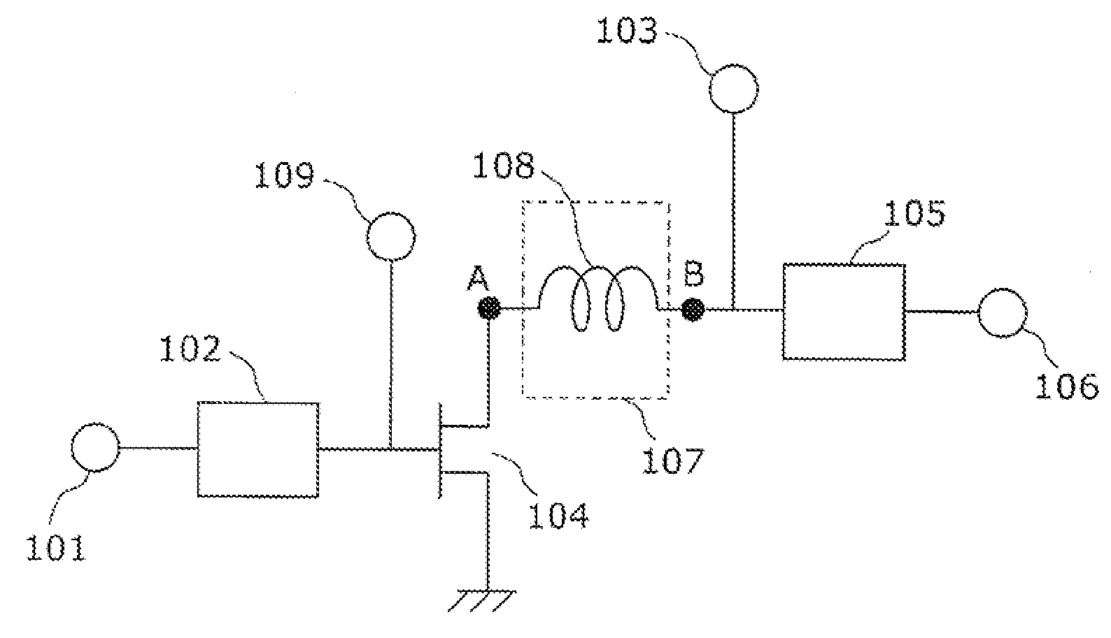
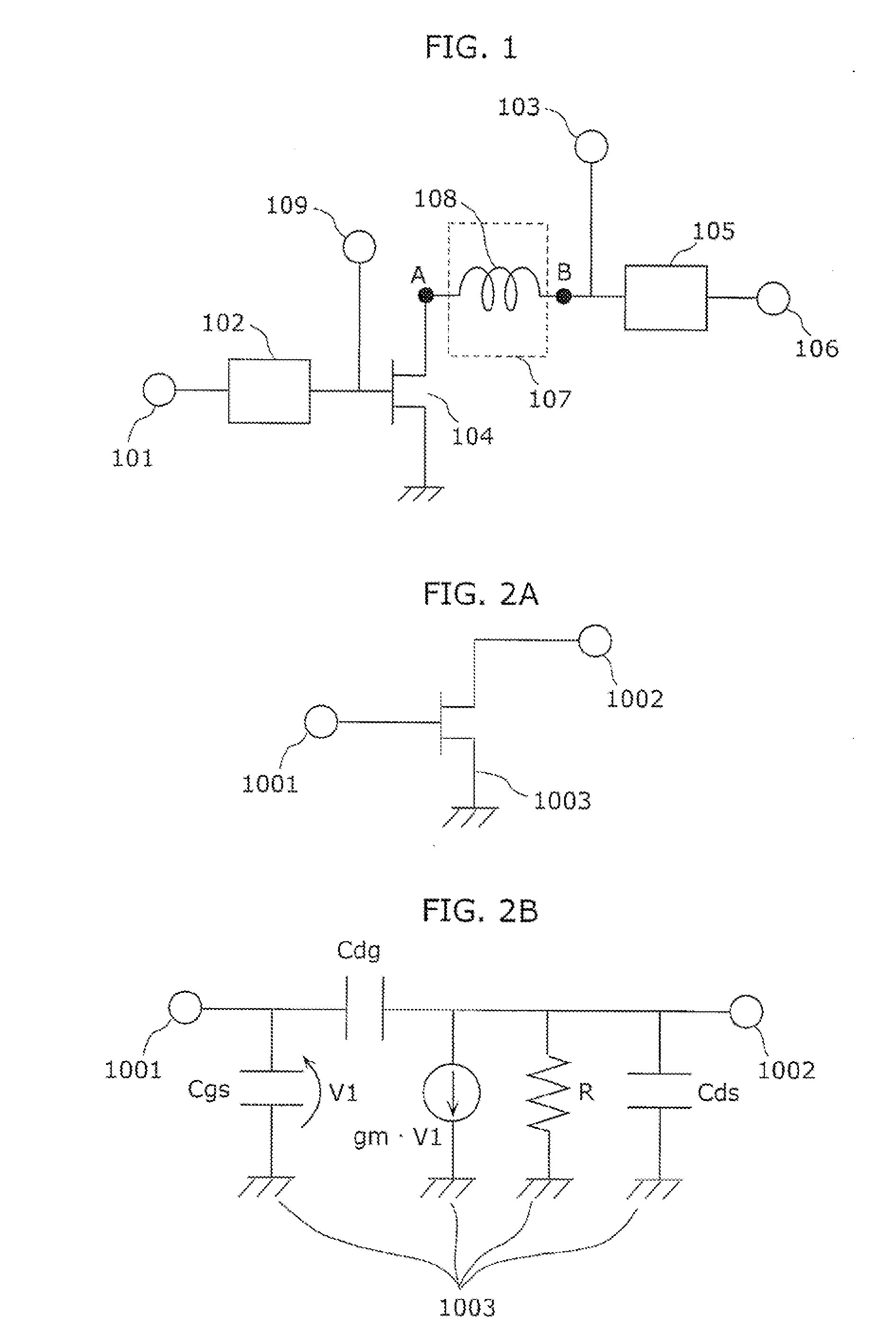
[0054]FIG. 1 shows a circuit diagram of a radio frequency power amplifier according to a first embodiment of the present invention.

[0055]As shown in FIG. 1, the radio frequency power amplifier according to a first embodiment of the present invention has an input matching circuit 102, a transistor 104 which is an amplifying element, a reactance control circuit 107, and an output matching circuit 105. An input terminal 101 of the radio frequency signal is connected to an input side of an input matching circuit 102, and a bias terminal 109 is connected to an output side of the input matching circuit 102. Direct current voltage to drive the transistor 104 is applied to a gate electrode of the transistor 104 via the bias terminal 109. Also, a bias terminal 103 is connected to an input side of an output matching circuit 105. Direct current voltage to drive the transistor 104 is applied to a drain electrode of the transistor 104 via the bias terminal 103. Furthermore, an output terminal 10...

Example

Second Embodiment

[0087]Next, FIG. 10 will be used to describe a second embodiment of a radio frequency power amplifier. FIG. 10 is a circuit diagram showing the second embodiment of a radio frequency power amplifier.

[0088]The difference between the first embodiment and the second embodiment of a radio frequency power amplifier is in the configuration of the reactance control circuit 107. Specifically, a microstrip line 401 is used as the reactance control circuit 107 in the second embodiment. Due to the fact that all other circuit configurations are identical to those of the first embodiment, and the components that are the same in FIG. 10 and FIG. 1 use the same reference signs, those descriptions will be omitted.

[0089]In the second embodiment, the reactance component can be adjusted depending on the line length and the characteristic impedance of the microstrip line 401 that forms the reactance control circuit 107. Therefore, as with the first embodiment, the line length and the c...

Example

Third Embodiment

[0090]Next, FIG. 11 will be used to describe a third embodiment of a radio frequency power amplifier. FIG. 11 is a circuit diagram showing the third embodiment of a radio frequency power amplifier.

[0091]The difference between the first embodiment and the third embodiment of a radio frequency power amplifier is in the configuration of the reactance control circuit 107. Specifically, a series resonant circuit including an inductor 501 and a capacitor 502 is used as the reactance control circuit 107 in the third embodiment. Due to the fact that all other circuit configurations are identical to those of the first embodiment, and the components that are the same in FIG. 11 and FIG. 1 use the same reference signs, those descriptions will be omitted.

[0092]Here, resonance frequency is defined as F, the parasitic capacitance of transistor 104 is defined as C, the inductance of inductor 501 in the reactance control circuit is defined as L, and the capacitance of capacitor 502 ...


PUM


Abstract

A radio frequency power amplifier having a transistor 104 that amplifies a radio frequency signal of a first frequency; an input matching circuit 102 connected to an input terminal of the transistor 104; an output matching circuit 105 connected to an output terminal of the transistor 104; and a reactance control circuit 107 with one end connected to the output terminal of the transistor 104, and the other end connected to an input terminal of an output matching circuit 105 and a bias terminal 103. The reactance control circuit 107 has a reactance which resonates at a second frequency with a parasitic capacitance of the transistor 104 at the output terminal of the transistor 104. The second frequency is identical or close to the first frequency.

Description

TECHNICAL FIELD[0001]The present invention relates to a radio frequency power amplifier, and, in particular, to a technique for increasing the efficiency of a high-power radio frequency power amplifier.BACKGROUND ART[0002]Radio frequency power amplifiers are devices which output an amplified input signal, and are widely used in mobile communication terminals and base stations. However, radio frequency power amplifiers require a large amount of power and consume most of the supplied power needed to drive radio frequency generator circuits or transmitter circuits, hindering the low power consumption of mobile communication terminals and base stations. Accordingly, there has long been a need for a radio frequency power amplifier with decreased driving power.[0003]A radio frequency power amplifier has input and output characteristics such that when the input power is low, the input signal is amplified while maintaining constant gain (in the linear region). As the input power increases, ...

Claims


Application Information

Patent Timeline
IPC IPC(8): H03F3/16
CPCH03F1/32H03F2203/7215H03F1/56H03F3/189H03F3/193H03F3/195H03F3/245H03F2200/108H03F2200/15H03F2200/18H03F2200/222H03F2200/387H03F2200/391H03F2200/423H03F1/3205
Inventor UNO, TAKASHIYAHATA, KAZUHIROISHIZAKI, TOSHIO
Owner PANASONIC SEMICON SOLUTIONS CO LTD
Why Eureka
Try Eureka