Semiconductor device and manufacturing method thereof

a technology of semiconductor devices and manufacturing methods, applied in semiconductor devices, electrical equipment, transistors, etc., can solve the problems of difficult control of circuits and unsuitable drain current flows, and achieve the effect of improving the reliability of transistors driven at high voltage or large currents

Active Publication Date: 2012-05-10
SEMICON ENERGY LAB CO LTD
View PDF2 Cites 44 Cited by
  • Summary
  • Abstract
  • Description
  • Claims
  • Application Information

AI Technical Summary

Benefits of technology

[0030]According to one embodiment of the present invention, the threshold voltage value of a transistor can be made to be positive, whereby a so-called normally-off switching element can be realized. Further, according to one embodiment of the present invention, the threshold voltage of a normally-on transistor can be made to be close to zero. Further, according to one embodiment of the present invention, the reliability of a transistor which is driven at high voltage or large current can be improved.

Problems solved by technology

When the threshold voltage value is negative even when the field effect mobility is high, it is difficult to control as the circuit.
Such a transistor in which a channel is formed even at a negative voltage so that a drain current flows is not suitable as a transistor used in a circuit.

Method used


Image

  • Semiconductor device and manufacturing method thereof
  • Semiconductor device and manufacturing method thereof
  • Semiconductor device and manufacturing method thereof

Examples


embodiment 1

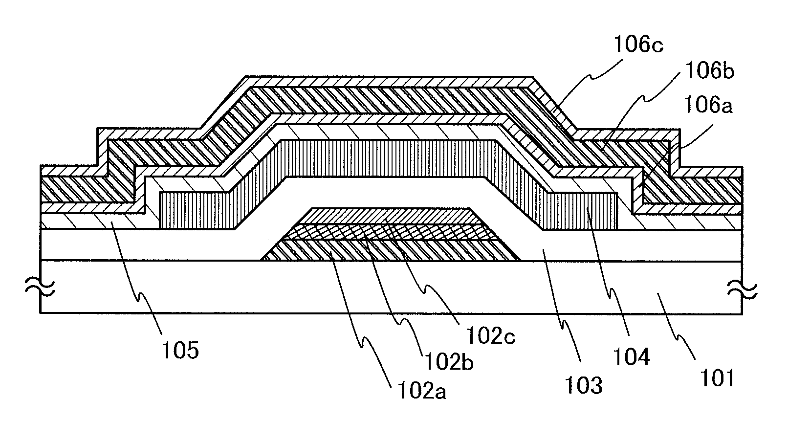
[0042]In this embodiment, an example of manufacturing a transistor over a substrate is described using FIGS. 1A to 1C.

[0043]First, a conductive film including three layers whose materials are different from one another is formed over a substrate 101, a resist mask is formed over the conductive film with a first photomask, and etching is performed selectively thereon, whereby a gate electrode layer is formed. After that, the resist mask is removed. If necessary, a base insulating film of a silicon oxide, a silicon nitride, a silicon oxynitride, a silicon nitride oxide, or the like may be provided ahead of formation of the conductive film.

[0044]As a material of the substrate 101, a glass material such as aluminosilicate glass, aluminoborosilicate glass, or barium borosilicate glass can be used. In the mass production, a mother glass with the following size is preferably used for the substrate 101: the 8-th generation (2160 mm×2460 mm); the 9-th generation (2400 mm×2800 mm, or 2450 mm×...

embodiment 2

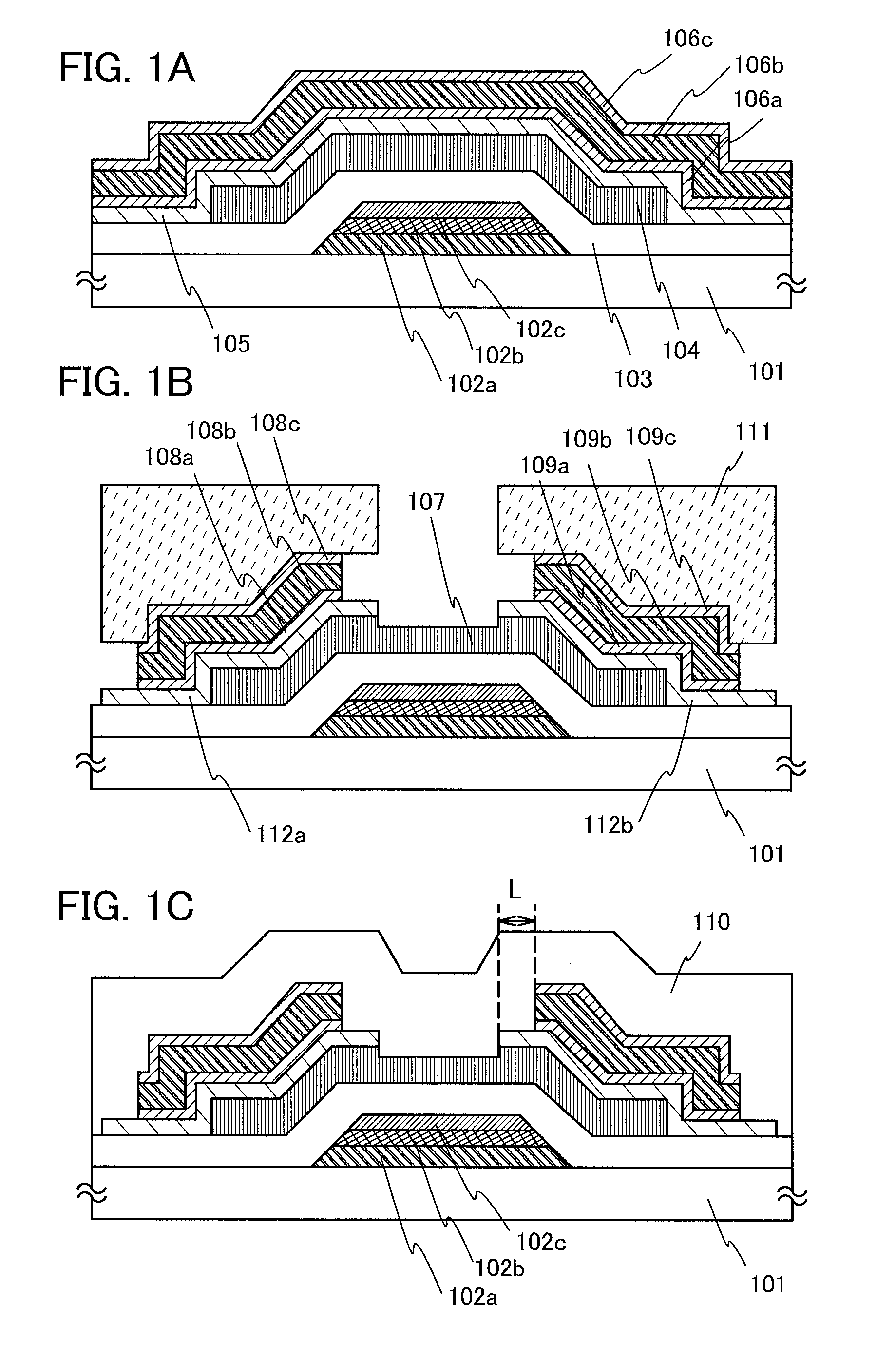
[0085]In this embodiment, an example of manufacturing a transistor and a pixel electrode with four photomasks in total which is smaller than the number of photomasks in Embodiment 1 by one is described using FIG. 4 and FIGS. 5A to 5D. In this embodiment, the manufacturing of the transistor is different from Embodiment 1 just in part thereof; thus, detailed description of the same portion is omitted in this embodiment.

[0086]FIG. 4 is a top view illustrating a plan structure of a pixel 310, and FIGS. 5A to 5D are cross-sectional views illustrating a stacked-layer structure of the pixel 310. Chain lines A1-A2, B1-B2, C1-C2, and D1-D2 in FIG. 4 correspond to cross sections A1-A2, B1-B2, C1-C2, and D1-D2 in FIGS. 5A to 5D, respectively.

[0087]In a transistor 311 described in this embodiment, a drain electrode layer 206b is partly surrounded by a U-shaped (C-shaped or horseshoe-shaped) source electrode layer 206a. With such a shape, a sufficient channel width can be ensured even when the a...

embodiment 3

[0102]Described in Embodiments 1 and 2 are an example of a bottom gate transistor. In this embodiment, an example of manufacturing a top gate transistor is described. In FIGS. 6A to 6C, the same portions as those shown in FIGS. 1A to 1C are denoted by the same reference numerals.

[0103]Further, according to this embodiment, an oxide semiconductor layer is formed by deposition two times.

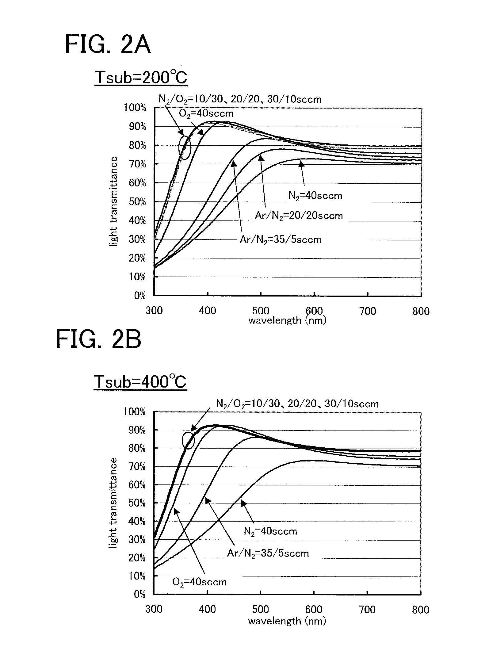
[0104]First, an oxide insulating film 160 which serves as a base insulating layer is formed over a substrate 101.

[0105]The oxide insulating film 160 is formed using an oxide insulating film from which part of oxygen is released by heat treatment. The oxide insulating film which contains oxygen over the stoichiometric proportion is preferably used as the oxide insulating film from which part of oxygen is released by heat treatment. With the oxide insulating film from which part of oxygen is released by heat treatment, oxygen can be diffused into a crystalline oxide semiconductor film by heat treatment. ...


PUM


Abstract

A semiconductor device having a novel structure or a method for manufacturing the semiconductor device is provided. For example, the reliability of a transistor which is driven at high voltage or large current is improved. For improvement of the reliability of the transistor, a buffer layer is provided between a drain electrode layer (or a source electrode layer) and an oxide semiconductor layer such that the end portion of the buffer layer is beyond the side surface of the drain electrode layer (or the source electrode layer) when seen in a cross section, whereby the buffer layer can relieve the concentration of electric field. The buffer layer is a single layer or a stacked layer including a plurality of layers, and includes, for example, an In—Ga—Zn—O film containing nitrogen, an In—Sn—O film containing nitrogen, an In—Sn—O film containing SiOx, or the like.

Description

BACKGROUND OF THE INVENTION[0001]1. Field of the Invention[0002]An embodiment of the present invention relates to a semiconductor device including a transistor or including a circuit including a transistor. For example, an embodiment of the present invention relates to a semiconductor device including a transistor in which a channel formation region is formed using an oxide semiconductor or including a circuit including such a transistor.[0003]2. Description of the Related Art[0004]A technique for manufacturing a transistor or the like using an oxide semiconductor film for a channel formation region to apply to a display device has been attracting attention. Examples of such a transistor include a transistor in which zinc oxide (ZnO) is used as an oxide semiconductor film and a transistor in which InGaO3(ZnO)m is used as an oxide semiconductor film. A technique for manufacturing such a transistor including an oxide semiconductor film over a light-transmitting substrate to apply to a...

Claims


Application Information

Patent Timeline
Patent Type & Authority Applications(United States)
IPC IPC(8): H01L29/786
CPCH01L27/1225H01L27/124H01L29/41733H01L29/45H01L29/78693H01L29/78618H01L29/78621H01L29/7869H01L29/263H01L29/4908H01L29/78603H01L29/04
Inventor YAMAZAKI, SHUNPEINONAKA, YUSUKEOMATA, TAKATSUGUHONDA, TATSUYAMIYANAGA, AKIHARUOHARA, HIROKI
Owner SEMICON ENERGY LAB CO LTD
Why Eureka
Try Eureka