Organic semiconductors as window layers for inorganic solar cells

a solar cell and organic semiconductor technology, applied in the field of organic semiconductors, can solve the problems of difficult and expensive production of efficient crystalline-based devices, low voc, and inability to provide signal or current to control detection circuitry, etc., and achieve the effect of increasing power conversion and increasing vo

Active Publication Date: 2012-05-17
RGT UNIV OF MICHIGAN
View PDF5 Cites 1 Cited by
  • Summary
  • Abstract
  • Description
  • Claims
  • Application Information

AI Technical Summary

Benefits of technology

[0024]The present disclosure relates to a device comprising: an anode; a cathode; an inorganic substrate; and at least one organic window layer. In one embodiment, the device comprises at least one inorganic epilayer. The organic window layer disclosed herein is positioned between the anode and cathode, such as between an inorganic semiconductor layer and a contact, including between the anode and the at least one inorganic epilayer. In one embodiment, the disclosed device exhibits one or more of the following characteristics when compared to the device without the at least one organic window layer: increased VOC at one sun AM1.5G illumination; increased power conversion at one sun AM1.5G illumination; enhanced Schottky barrier height; or reduced forward dark current.

Problems solved by technology

As a general rule, a photovoltaic cell provides power to a circuit, device or equipment, but does not provide a signal or current to control detection circuitry, or the output of information from the detection circuitry.
In contrast, a photodetector or photoconductor provides a signal or current to control detection circuitry, or the output of information from the detection circuitry but does not provide power to the circuitry, device or equipment.
However, efficient crystalline-based devices, especially of large surface area, are difficult and expensive to produce due to the problems inherent in producing large crystals without significant efficiency-degrading defects.
On the other hand, high efficiency amorphous silicon devices still suffer from problems with stability.
The maximum total power generated by a PV device is inherently incapable of exceeding the product, ISC×VOC.
Such a process can be induced by the built-in electric field, but the efficiency at the electric fields typically found in organic devices (F ˜106 V / cm) is low.
However, organic PV devices typically have relatively low external quantum efficiency (electromagnetic radiation to electricity conversion efficiency), being on the order of 1% or less.
The materials currently used for the window layers or hetero-contact layers have been limited to inorganic semiconductors and dielectrics.

Method used


Image

  • Organic semiconductors as window layers for inorganic solar cells
  • Organic semiconductors as window layers for inorganic solar cells
  • Organic semiconductors as window layers for inorganic solar cells

Examples


example

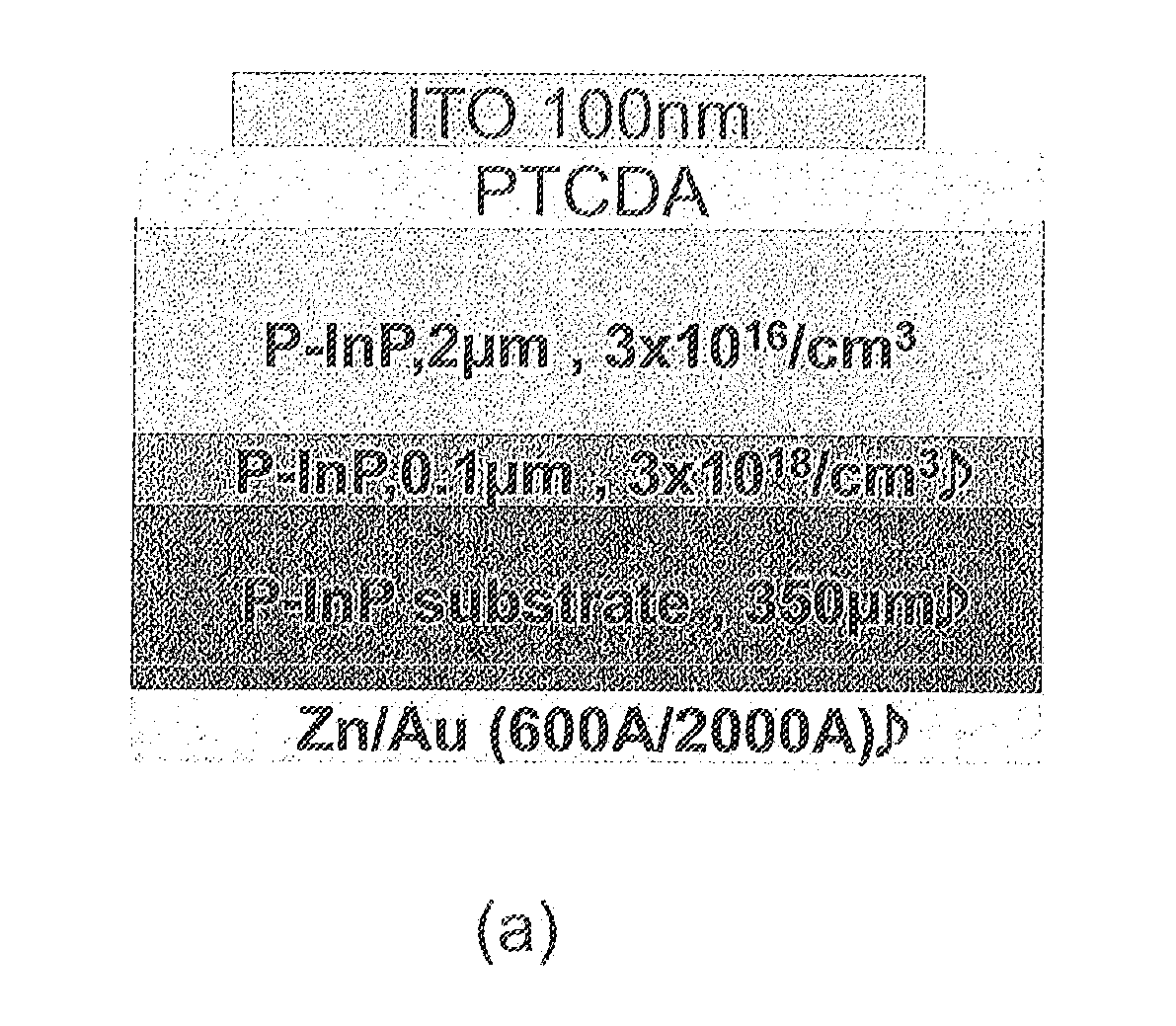
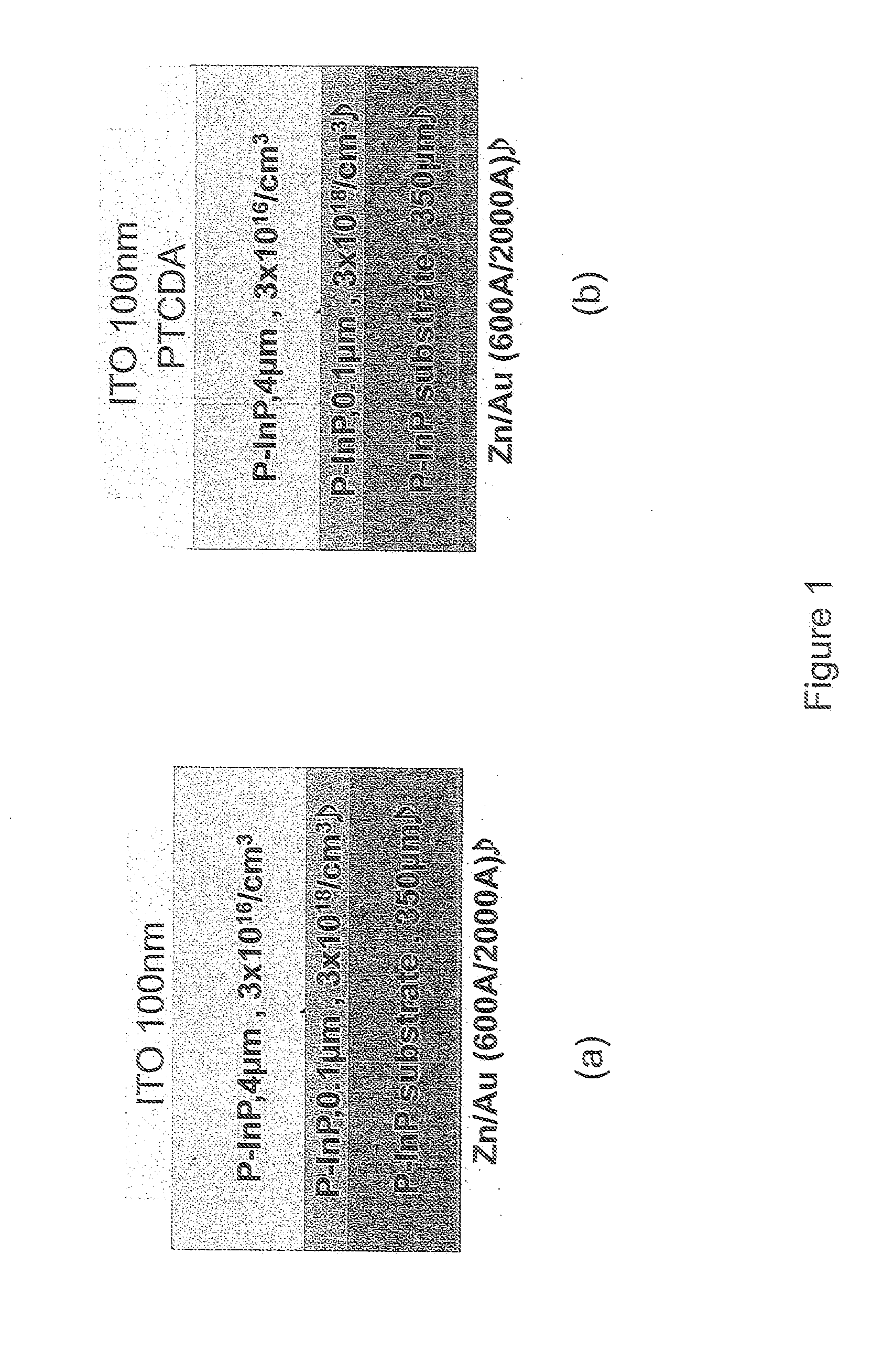
[0082]The epitaxial solar cell structure was grown by gas source molecular beam epitaxy on a p-type, Zn-doped (100) InP substrate. The epitaxial structure consisted of a 0.1 μm thick, Be doped (3×1018 cm−3) p-type InP buffer layer and a 4 μm thick lightly Be doped (3×1016 cm−3) p-type InP absorption layer.

[0083]The epitaxial wafer was then fabricated into Schottky barrier solar cells both without PTCDA window layer and with PTCDA window layer. Right before the device processing, the surface of the InP epi-wafer was treated with one minute of NR4OH dip to remove the native oxide.

[0084]To make the conventional InP Schottky barrier solar cells, indium-tin-oxide (ITO) electrode was directly sputtered on top of the surface-treated InP epi-wafer to form the structure shown in FIG. 1(a). To make the devices with PTCDA window layer, a thin layer of PTCDA was deposited first using vacuum thermal evaporation on the surface-treated InP epi-wafer. ITO electrode was then sputtered on top of the ...


PUM


Abstract

Disclosed is a device comprising: an anode; a cathode; an inorganic substrate; and at least one organic window layer positioned between: the anode and the inorganic substrate; or the cathode and the inorganic substrate. Also disclosed is a method of enhancing the performance of a photosensitive device having an anode, a cathode, and an inorganic substrate, comprising: positioning at least one organic window layer between the anode and the cathode. In one embodiment the organic window layer may absorb light and generate excitons that migrate to the inorganic where they convert to photocurrent, thereby increasing the efficiency of the device. Also disclosed is a method of enhancing Schottky barrier height of a photosensitive device, the method being substantially similar to the previously defined method.

Description

CROSS-REFERENCE TO RELATED APPLICATIONS[0001]This application claims the benefit of U.S. Provisional Application No. 61 / 382,885, filed Sep. 14, 2010, the disclosure of which is incorporated herein by reference.STATEMENT REGARDING FEDERALLY SPONSORED RESEARCH[0002]The subject matter of this application was prepared with U.S. Government support under Contract No. DE-SC0001011 awarded by the Department of Energy. The government has certain rights in the subject matter of this application.JOINT RESEARCH AGREEMENT[0003]The subject matter of this application was made by, on behalf of, and / or in connection with one or more of the following parties to a joint university-corporation research agreement: University of Michigan and Global Photonic Energy Corporation. The agreement was in effect on and before the date the claimed invention was made, and the claimed invention was made as a result of activities undertaken within the scope of the agreement.BACKGROUND[0004]Optoelectronic devices rel...

Claims


Application Information

Patent Timeline
Patent Type & Authority Applications(United States)
IPC IPC(8): H01L51/44H01L51/48H01L51/46
CPCH01L31/07H01L31/184Y02E10/549H01L51/4213Y02E10/544H01L51/0053H10K85/621H10K30/10H10K30/50H01L31/04H01L31/0224H01L31/0304
Inventor FORREST, STEPHEN R.LI, NING
Owner RGT UNIV OF MICHIGAN
Why Eureka
Try Eureka