Charge-transporting material and organic electroluminescence device

Inactive Publication Date: 2012-05-24
UDC IRELAND
View PDF5 Cites 393 Cited by
  • Summary
  • Abstract
  • Description
  • Claims
  • Application Information

AI Technical Summary

Benefits of technology

[0069]According to the invention, an organic electroluminescence device hav

Problems solved by technology

In general, one organic compound material contains two or more kinds of halogen-containing impurities but not all of them equally influence the durability of organic electroluminescence device using the organic compound material, and it is not easily known that what a structure of haloge

Method used


Image

  • Charge-transporting material and organic electroluminescence device
  • Charge-transporting material and organic electroluminescence device
  • Charge-transporting material and organic electroluminescence device

Examples


example 1

Synthesis of Exemplified Compound 1

(Synthesis Method B: Comparative Synthesis Method)

[0331]Exemplified compound 1 of the charge-transporting material represented by formula (1) was synthesized and purified according to the method described in WO 05 / 085387, paragraphs [0074] to [0075]. The reaction formulae are shown below.

[0332]The obtained sample was subjected to sublimation purification (heating at 5×10⁻¹ Pa under Ar flow), and fractions A, B and C were portioned out from the settled position of the sample at the time of recovery, from which each charge-transporting material was obtained. Fraction B is a region farther than fraction A and fraction C is a region farther than fraction B from the settled position of the sample. A material capable of vaporizing at a lower temperature is recovered from fraction B as compared with fraction A, and from fraction C as compared with fraction B.

[0333]Purification by HPLC and the contents of specific impurities of the obtained charge-transpor...

example 2

Manufacture of Device

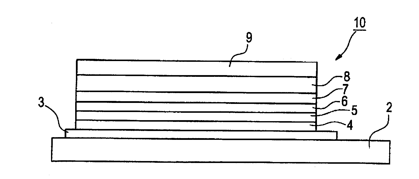
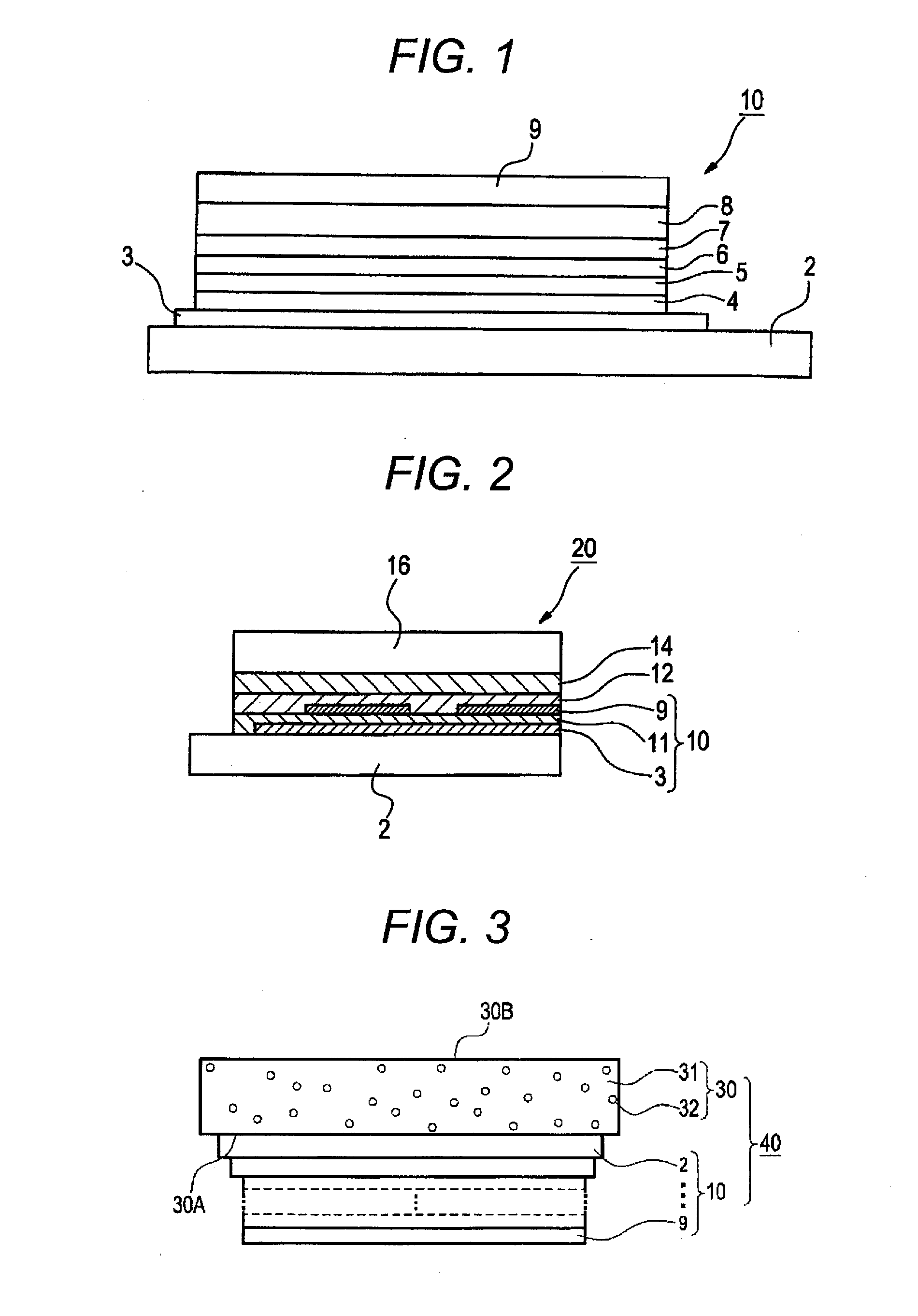
[0340]A glass substrate having an ITO film (manufactured by Geomatec Co., Ltd., surface resistance: 10Ω / □)) having a thickness of 0.5 mm and a size of 2.5 cm square was put in a washer and subjected to ultrasonic washing in 2-propanol, and then UV-ozone treatment for 30 minutes. The organic compound layers shown below were deposited on the transparent anode (ITO film) in sequence by a vacuum deposition method.

First Layer: 2-TNATA and F4-TCNQ (mass ratio: 99.7 / 0.3); film thickness: 120 nm

Second Layer: α-NPD; film thickness: 7 nm

Third Layer: C-1; film thickness: 3 nm

Fourth Layer: H-1 and D-1 (mass ratio: 85 / 15); film thickness: 30 nm

Fifth Layer Electron-transporting material (the charge-transporting material manufactured in Example 1, shown in Tables 1 and 2); film thickness: 3 nm

Sixth Layer: BAlq; film thickness: 27 nm

[0341]Lithium fluoride in a thickness of 0.1 nm and metal aluminum in a thickness of 100 nm were deposited thereon in this order to obtain a cathod...

example 3

Manufacture of Device

[0349]Each device was manufactured in the same manner as in Example 2 except for carrying out deposition of the organic compound layers in the order of the following first layer to fifth layer.

First Layer: 2-TNATA and F4-TCNQ (mass ratio: 99.7 / 0.3); film thickness: 120 nm

Second Layer: α-NPD; film thickness: 7 nm

Third Layer: C-1; film thickness: 3 nm

Fourth Layer Host material as shown in Tables 3 and 4 (the charge-transporting material manufactured in Example 1) and light-emitting material (mass ratio: 95 / 5); film thickness: 30 nm

Fifth Layer: BAlq; film thickness: 30 nm

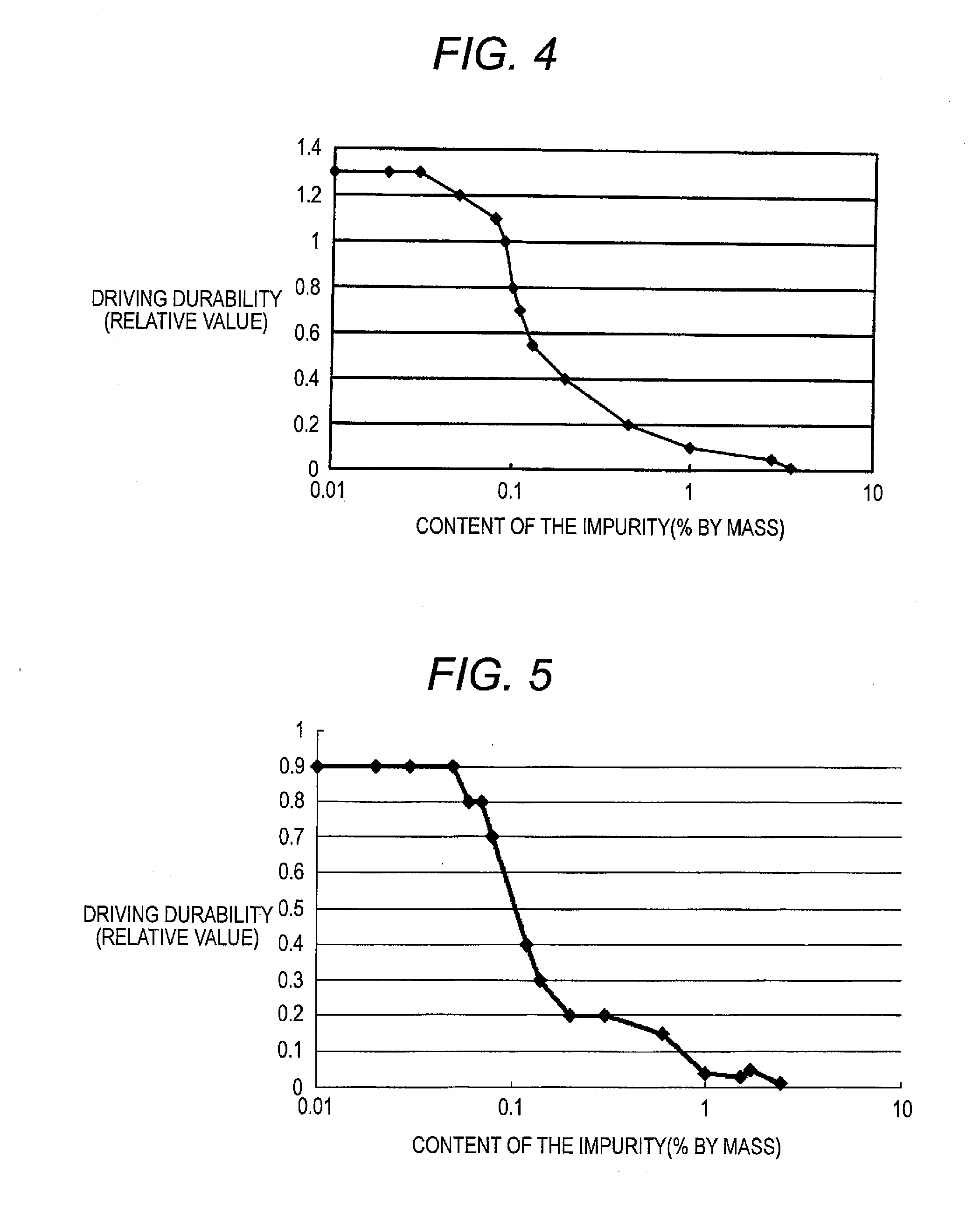
[0350]As a result of light emission of these devices, light emission resulting from the used light-emitting material was obtained from each device. Performances of each obtained device were evaluated by measuring external quantum efficiency and driving durability in the same manner as in Example 2. The results obtained are shown in Tables 3 and 4.

[0351]Concerning the value of driving durability sho...


PUM


Abstract

A charge-transporting material contains a compound represented by the following formula (1) in an organic layer, in which the contents of specific halogen-containing compounds are 0.1% or less to the compound represented by formula (1). In formula (1), each of A1 and A2 independently represents N, —CH or —CR; R represents a substituent; L represents a single bond, an arylene group, a cycloalkylene group or an aromatic heterocyclic group; each of R1 to R5 independently represents a substituent; each of n1, n2 and n3 independently represents an integer of 0 to 4; each of n4 and n5 independently represents an integer of 0 to 5; and each of p and q independently represents an integer of 1 to 4.

Description

TECHNICAL FIELD[0001]The present invention relates to a charge-transporting material and an organic electroluminescence device.BACKGROUND ART[0002]Since organic electroluminescence devices (hereinafter also referred to as “devices” or “organic EL devices”) are capable of obtaining high luminance emission of light by low voltage driving, they are actively researched and developed. An organic electroluminescence device comprises a pair of electrodes and an organic layer between the pair of electrodes, electrons injected from the cathode and holes injected from the anode are recombined in the organic layer, and generated energy of exciton is used for emission of light.[0003]In recent years, increment in efficiency of devices has been advanced by the use of phosphorescent materials. Doping type devices using a light emitting layer including a host material doped with a light emitting material are also widely adopted.[0004]For example, in patent documents 1 to 3 are proposed organic elec...

Claims


Application Information

Patent Timeline
IPC IPC(8): H01L51/54C07D403/14C07D401/10C07D403/10
CPCC07D403/10H01L51/0067H01L51/5048H01L51/0085H01L51/0072H10K85/654H10K85/6572H10K85/342H10K50/14C09K2211/1059C09K2211/1029C09K2211/1044
Inventor KITAMURA, TETSUWATANABE, TORUISE, TOSHIHIROTAKIZAWA, HIROO
Owner UDC IRELAND
Why Eureka
Try Eureka