
Apparatus and method for controlling power gating in an integrated circuit

Active Publication Date: 2012-05-24
ARM LTD
View PDF2 Cites 16 Cited by
  • Summary
  • Abstract
  • Description
  • Claims
  • Application Information

AI Technical Summary

Benefits of technology

[0016]Such an approach provides an adaptive technique for determining the appropriate control voltage to provide to the power gating circuitry, with the aim of reducing the leakage current to an acceptable level, whilst avoiding undue wear out of the power gating circuitry by only providing a control voltage sufficient to achieve the desired leakage current. Through use of such a technique, the control voltage can readily be varied having regard to operating conditions. For example, the higher the operating temperature of the integrated circuit, the greater the leakage current will be. Hence, as the operating temperature increases, the control voltage will need to be varied to seek to bring the leakage current down to an acceptable level. Conversely, if the integrated circuit is running at a low temperature, the leakage current will be less, and may drop below a threshold level that would have been acceptable. In such cases, the control voltage can be changed in order to increase the leakage current, with the aim of reducing wear out of the components within the power gating circuitry.
[0018]Hence, in one such embodiment, when the operating parameter data indicates that the leakage current is exceeding the desired leakage current, the adaptive controller is arranged to set the feedback control signal to a value that causes the voltage regulator circuitry to increase the overdrive voltage provided a maximum predetermined voltage level has not been reached. Similarly, when the operating parameter data indicates that the leakage current is below the desired leakage current, the adaptive controller is arranged to set the feedback control signal to a value that causes the voltage regulator circuitry to decrease the overdrive voltage provided a minimum predetermined voltage level has not been reached. By such an approach, it can be seen that the voltage regulator circuitry in combination with the adaptive controller serve to make the leakage current converge on a desired leakage current. Hence, excessive leakage current is prevented by increasing the overdrive voltage, and conversely the overdrive voltage can be reduced in order to reduce wear out of the power gating circuitry when the leakage current is low enough to allow, i.e. where the leakage current is below the desired leakage current. This enables a balance to be achieved between suppressing leakage current and maximising life of the circuitry.
[0020]Whilst the desired leakage current could be specified to be a specific current value, in one embodiment the desired leakage current is specified as a range of leakage current values, thereby enabling the above described convergence to more readily be achieved.
[0021]The adaptive controller can take a variety of forms. However, in one embodiment the adaptive controller comprises a state machine that is enabled when said low power mode is entered, the state machine transitioning between a plurality of states dependent on the received operating parameter data. The use of a state machine to provide the functionalities of the adaptive controller provides a particularly efficient mechanism for achieving the required functionality of the adaptive controller.
[0028]Alternatively, or in addition, the monitoring circuits may comprise process skew monitoring circuitry for monitoring speed of operation of the block of components during the normal mode of operation. In particular, variations in the silicon on which the integrated circuits are produced will mean that some circuits inherently operate more quickly than other circuits. Process skew monitoring circuitry can determine whether a silicon is fast silicon (i.e. the integrated circuit is operating more quickly than the norm) or slow silicon (i.e. the integrated circuit is operating more slowly than the norm), and this information can be used to determine how to adjust the control voltage. In particular, components constructed on slow silicon have less leakage current than the same components constructed on fast silicon, and hence for an integrated circuit of the slow silicon type, a lower control voltage may be required to achieve the desired level of leakage current. By setting the control voltage to that lower level, the lifetime of the integrated circuit can be increased.

Problems solved by technology

In particular, with leading edge nanometer technology, the individual components are becoming significantly smaller in size, and the decrease in size is giving rise to a significant increase in power consumption due to leakage current, leakage current being the current that is drawn by a component when it is in theory turned off.
However, a side effect of such scaling is that the threshold voltage and channel length of the transistors need to be lowered to prevent speed degradation, and this lowering of the threshold voltage makes the transistors more leaky, i.e. the leakage current increases as the threshold voltage decreases.
However, whilst such power gating techniques have traditionally given rise to significant energy savings, the ability for such power gating techniques to achieve significant energy savings is being compromised in integrated circuits based on leading edge nanometer technology, due to the reduced size of the components, and the associated increase in leakage current.
Accordingly, it is found that when the transistors in the power gating circuitry are turned off in order to isolate the block of components from the source voltage supply, those transistors are in fact not fully turned off, and significant leakage current through them can occur.
This in turn results in the block of components itself not being fully powered down, and accordingly further leakage current being drawn by those components.
However, blocks of components may be power gated for significant amounts of time, which means that such power gating transistors are exposed to a gate voltage that exceeds the source voltage supply for significant periods of time.
This is undesirable, as such increased gate voltages serve to reduce the operational life (increase “wear out”) of the transistors by slowly increasing their threshold voltage.

Method used


Image

  • Apparatus and method for controlling power gating in an integrated circuit
  • Apparatus and method for controlling power gating in an integrated circuit
  • Apparatus and method for controlling power gating in an integrated circuit

Examples


Embodiment Construction

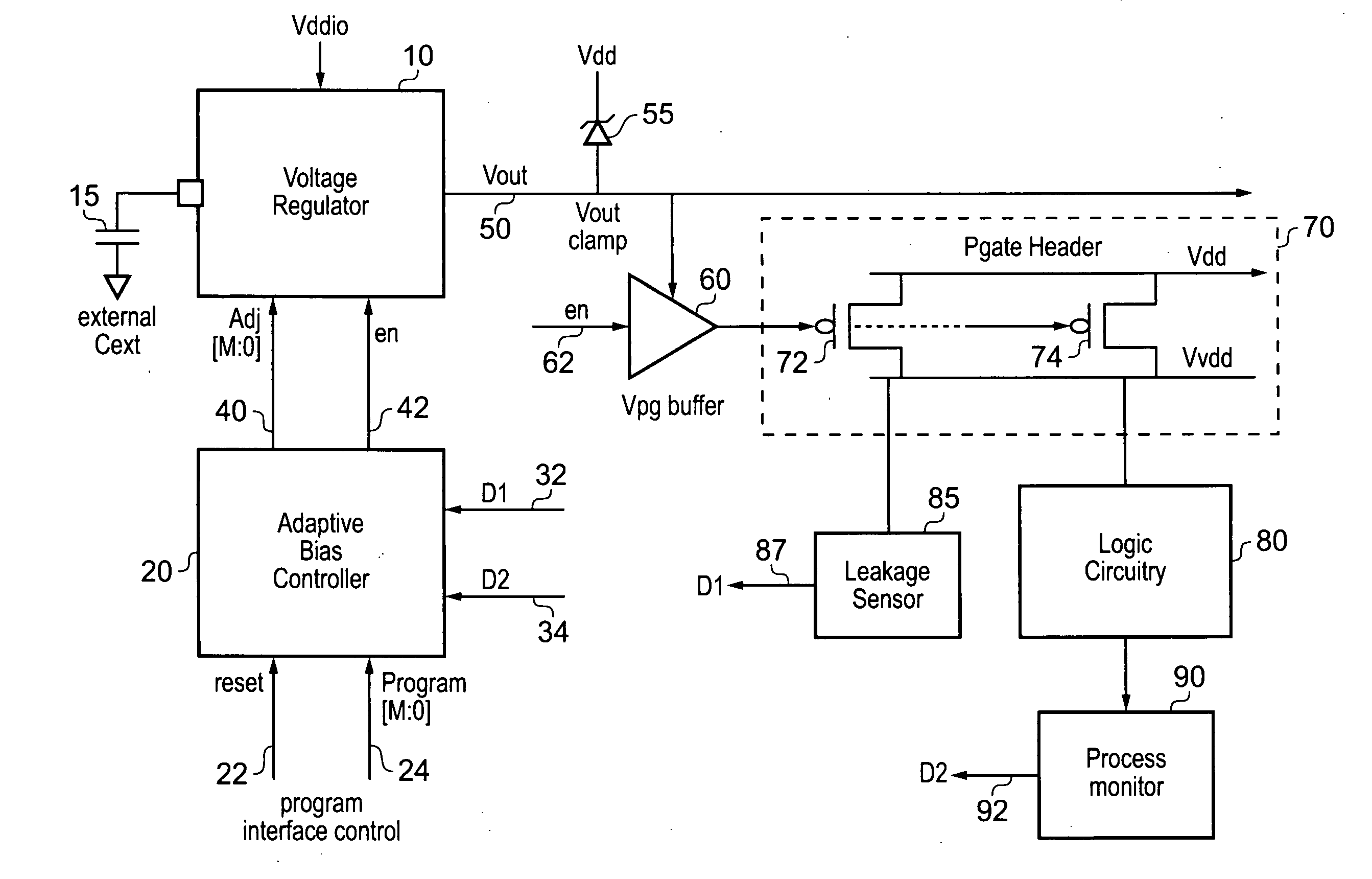
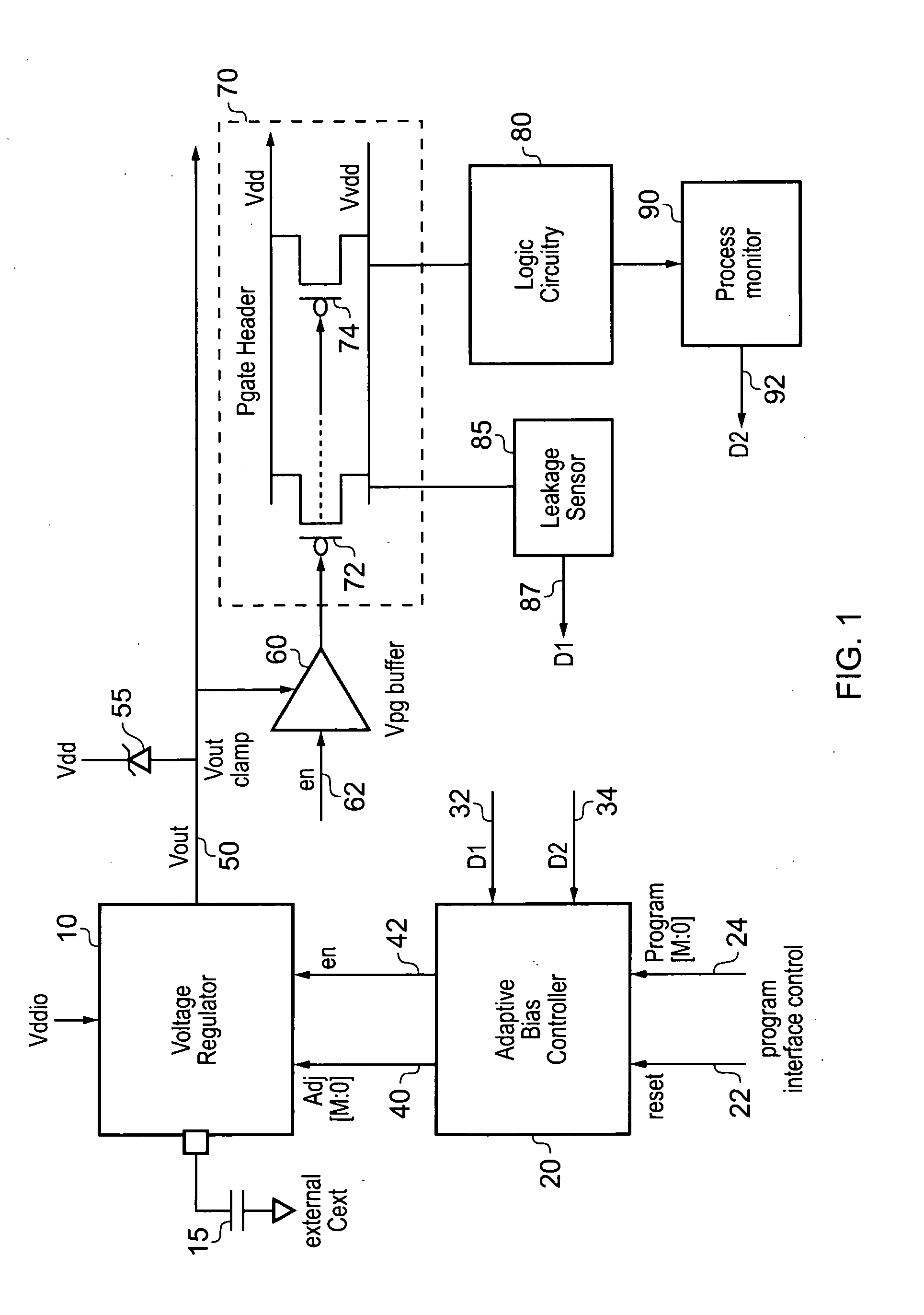
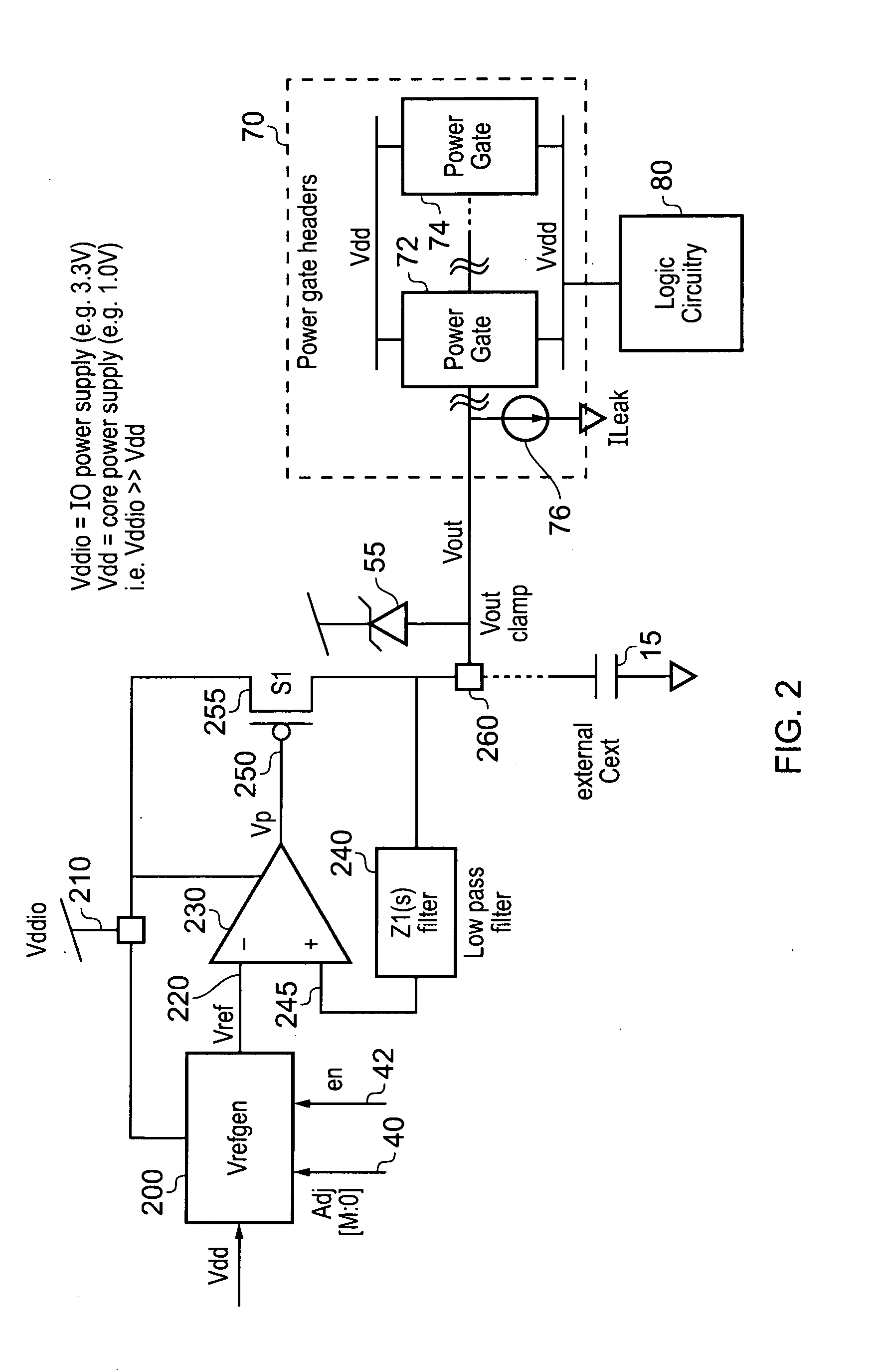
[0037]FIG. 1 is a block diagram of an integrated circuit in accordance with one embodiment. As shown in FIG. 1, an adaptive power controller 20 (referred to in FIG. 1 as an adaptive bias controller) is used to control the voltage regulator 10 to produce an output voltage which is used to drive the gates of transistors 72, 74 within a power gate header block 70 when the logic circuitry 80 is being placed in a power saving mode of operation. In particular, in the power saving mode of operation, the voltage regulator 10 produces an output voltage which is transferred by the buffer circuitry 60 to the gates of the transistor 72, 74 in order to turn those transistors off, thereby isolating the logic circuitry 80 from the voltage supply Vdd.

[0038]Various monitoring circuits 85, 90 are arranged to output operating parameter data to the adaptive bias controller 20, such operating parameter data being indicative of leakage current within the power gating circuitry 70. This operating paramete...


PUM


Abstract

A technique for controlling power gating in an integrated circuit is provided. The integrated circuit comprises a block of components to be power gated, and power gating circuitry for selectively isolating the block of components from the source voltage supply in order to achieve such power gating. Voltage regulator circuitry is used to provide a control voltage to the power gating circuitry when performing such power gating operations, the control voltage being settable to any of a plurality of predetermined voltage levels. An adaptive controller receives operating parameter data from either or both of the block of components and the power gating circuitry, that operating parameter data being indicative of leakage current. The adaptive controller then issues a feedback control signal to the voltage regulator circuitry whose value is dependent on the received operating parameter data. The voltage regulator circuitry is then responsive to the feedback control signal to change the control voltage between the plurality of predetermined voltage levels, until the operating parameter data indicates that a desired leakage current has been obtained within the power gating circuitry. Such an approach enables a balance to be achieved between reducing leakage current and reducing wear out of the power gating circuitry.

Description

BACKGROUND OF THE INVENTION[0001]1. Field of the Invention[0002]The present invention relates to an apparatus and method for controlling power gating in an integrated circuit.[0003]2. Description of the Prior Art[0004]Within an integrated circuit, it is known to employ adaptive power management or dynamic voltage scaling (DVS) techniques in order to reduce the power dissipation on a chip. Adaptive power management is becoming ever more important as process geometries decrease. In particular, with leading edge nanometer technology, the individual components are becoming significantly smaller in size, and the decrease in size is giving rise to a significant increase in power consumption due to leakage current, leakage current being the current that is drawn by a component when it is in theory turned off.[0005]As circuits become smaller and smaller due to technology scaling, the supply voltage to those circuits has to be reduced to reduce dynamic power consumption. However, a side effe...

Claims


Application Information

Patent Timeline
IPC IPC(8): H03K17/687
CPCH03K17/145H03K2017/066H03K19/00369H03K19/0008
Inventor SANDHU, BAL S.IDGUNJI, SATCHIN SATISHFLYNN, DAVID WALTER
Owner ARM LTD
Learn More