Microbolometer Semiconductor Material

a semiconductor material and microbolometer technology, applied in the field of infrared bolometer sensor material, can solve the problems of high noise characteristics, low sensitivity of components comprising such pn junctions, and inability to deposited monocrystalline and/or epitaxially deposited materials requiring high deposition temperatures on top of integrated circuits, etc., to achieve the effect of improving sensitivity and reducing nois

Active Publication Date: 2012-06-07
SENSIRION HLDG
View PDF3 Cites 11 Cited by
  • Summary
  • Abstract
  • Description
  • Claims
  • Application Information

AI Technical Summary

Benefits of technology

[0016]A bolometer as described herein may have an improved sensitivity and lower noise, compared to prior art bolometer st...

Problems solved by technology

However, a component comprising such PN junctions suffer from a low sensitivity and high noise characteristics.
However, the read-out electronic circuits of bolometers comprising such semiconductor structures have a very limited functionality since they must be placed beside the resistance ...

Method used


Image

  • Microbolometer Semiconductor Material
  • Microbolometer Semiconductor Material
  • Microbolometer Semiconductor Material

Examples


first embodiment

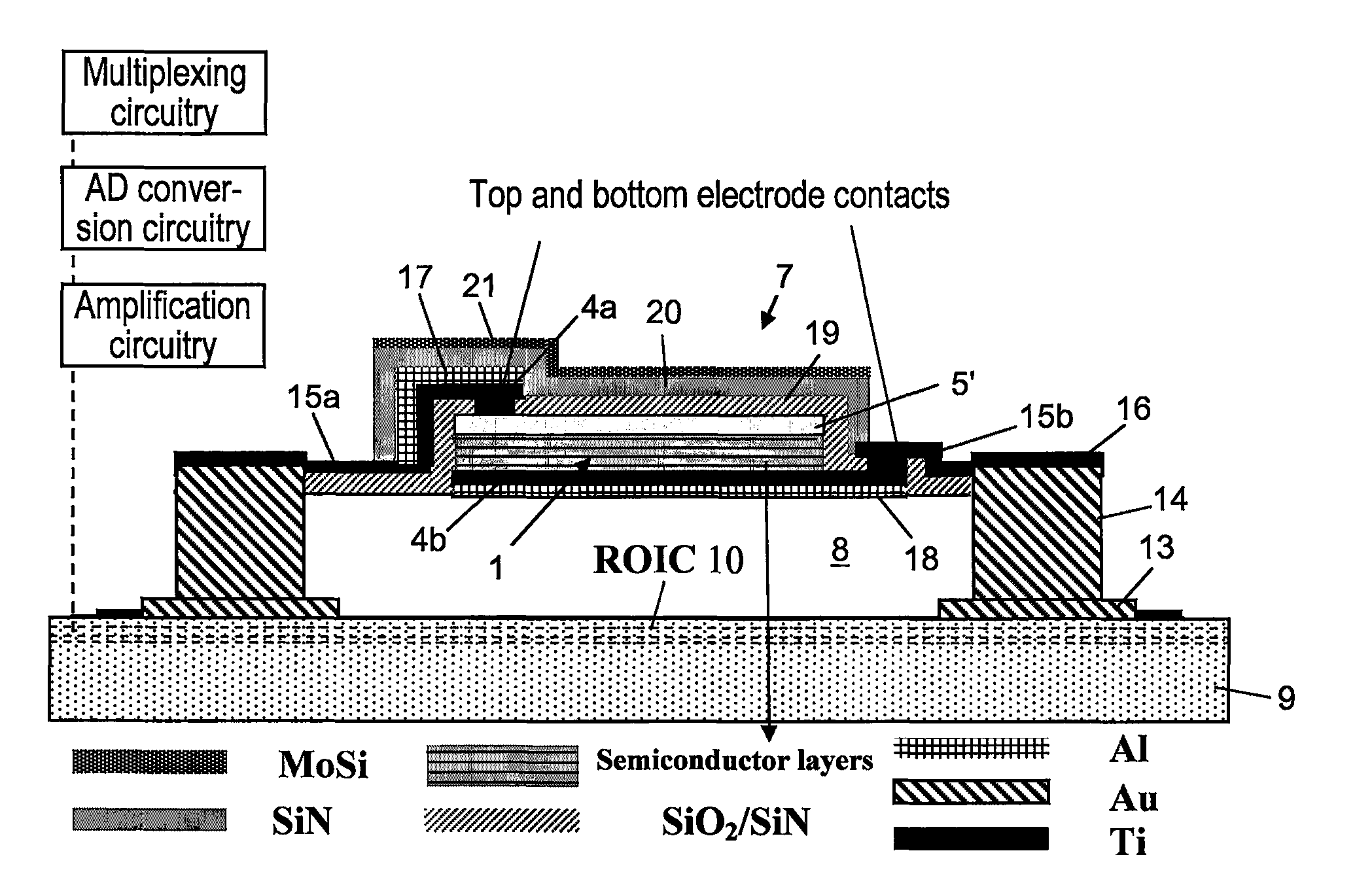
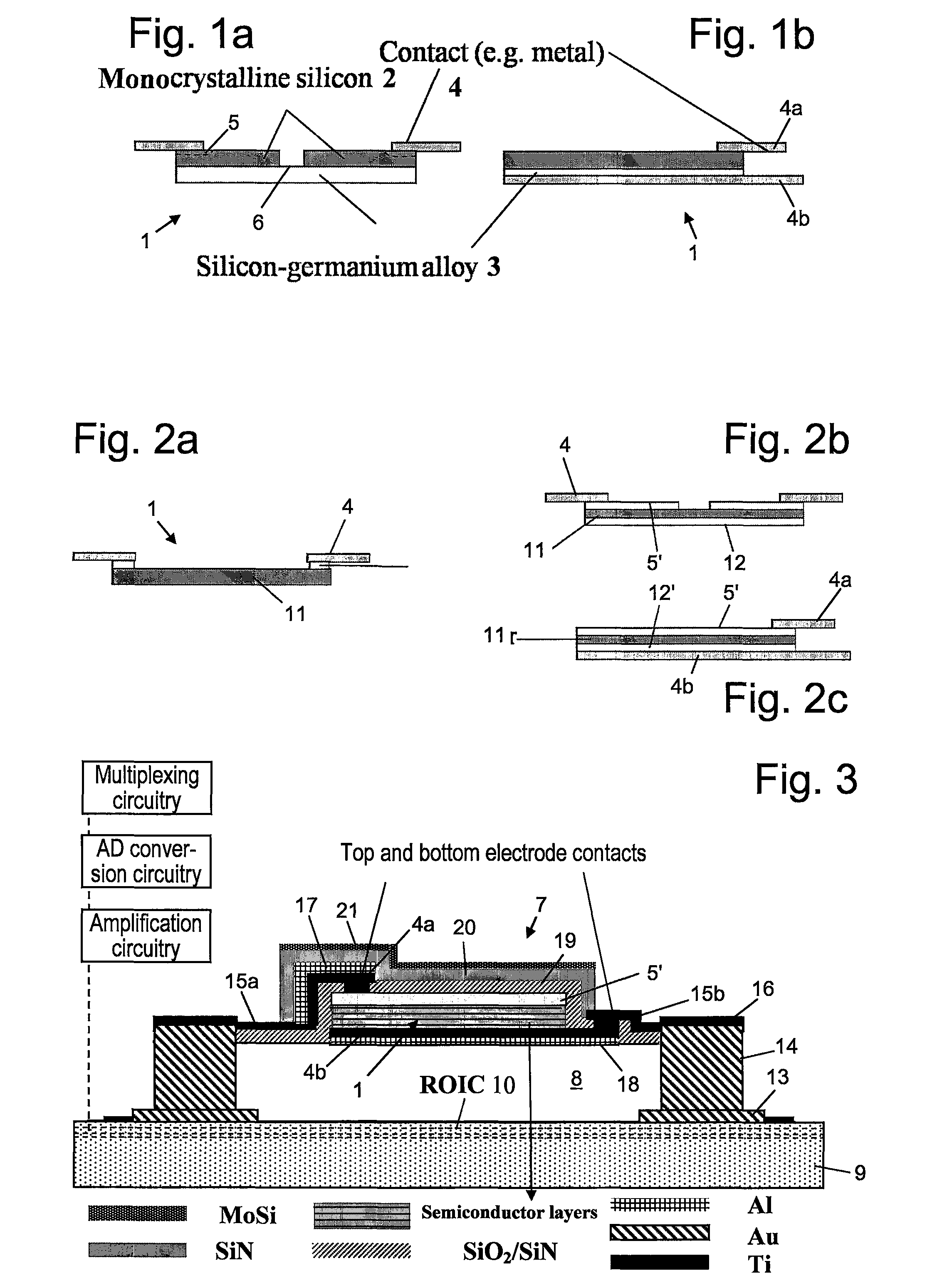
[0027]In a first embodiment, a bolometer based on semiconductor materials comprises as a resistance element 1 two layers, see FIGS. 1a and 1b, one silicon layer 2 and one silicon-germanium alloy layer 3, the layer having thermodynamically stable or at least meta-stable thicknesses and also the germanium concentration being thermodynamically stable Typical thicknesses are in the range of 10-100 nm and the atomic concentration of Ge is typically less than 40% and can even be less than e.g. 30%. The silicon-germanium layer 3 can be strained or unstrained. The silicon-germanium layer 3 is not intended to provide any quantum mechanical carrier confinement, known in the art as a quantum well (QW) or any alteration of the electronic band structure, other than strain-induced effects on e.g. the mobility and a band gap change, as generally expected for a given germanium concentration.

[0028]The concentration of the components of the silicon-germanium alloy in layer 3 can be constant in the la...

second embodiment

[0041]In a second embodiment, the resistor element 1 of a bolometer can comprise a single layer 11 of mono-crystalline silicon or of a silicon-germanium alloy as a temperature sensitive thermistor material, see FIGS. 2a, 2b and 2c. The silicon-germanium alloy can have the same composition as described above, i.e. containing less than 30 atomic % of Ge. The single layer 11 can be doped with one or more impurity dopants, the doping levels selected so that the layer retains the basic crystallographic properties of silicon, i.e. so that is not transformed to a poly-crystalline or amorphous state. The impurity dopants can be selected from the elements in groups III, N and V of the periodic table and in particular among boron, aluminium, indium, arsenic, phosphorous, antimony, germanium, carbon and tin. Typical doping levels are in the range from 1·1014 cm−3 until the level of solid solubility 1·1020 cm−3. The thermistor material may contain highly doped, e.g. p++, layers as electrical co...


PUM


Abstract

A sensor for detecting intensity of radiation such as of infrared radiation includes an ROIC substrate (9) and a resistance element (1) arranged at a distance of the surface of the ROIC substrate. The resistance element comprises one more semiconducting layers such as a silicon semiconducting layer and a semiconducting layer of a silicon-germanium alloy forming a heterojunction. The semiconducting layer or layers can be doped with one or more impurity dopants, the doping level or levels selected so that the layer retains the basic crystallographic properties of the respective material such as those of monosilicon or a monocrystalline silicon-germanium alloy. The impurity dopants are selected from the elements in groups IE, IV, and V, in particular among boron, aluminium, indium, arsenic, phosphorous, antimony, germanium, carbon and tin. The doping can be abrupt so that there is an interior layer inside said semiconducting layer or layers having a significantly higher doping level.

Description

RELATED APPLICATION[0001]This application claims priority and benefit from Swedish patent application No. 0900824-4, filed Jun. 17, 2009, the entire teachings of which are incorporated herein by reference.TECHNICAL FIELD[0002]The present invention relates to an infrared bolometer sensor material.BACKGROUND[0003]A bolometer comprises as a main element a component that changes its electrical resistivity or resistance when exposed to different temperatures, this component also called herein a resistance element. The component is mounted so that it absorbs radiation, e.g. visible light or infrared light, the intensity of which is to be detected. The component is connected to or in an electric circuit, sensing the resistance changes, the electric circuit called a read-out electronic circuit.[0004]The performance of infrared bolometers and infrared bolometer arrays for imaging applications can be significantly increased if said component comprises sensing devices based on semiconductor gr...

Claims


Application Information

Patent Timeline
IPC IPC(8): H01L29/66
CPCG01J5/02Y02E10/547G01J5/024G01J5/046G01J5/22H01L27/14649H01L31/022408H01L31/09H01L31/1035H01L31/108H01L31/1085H01L31/1804H01L31/1812H01L31/1892G01J5/0215Y02P70/50
Inventor MALM, GUNNAR
Owner SENSIRION HLDG
Why Eureka
Try Eureka