
Liquid organic semiconductor material

a semiconductor material and liquid organic technology, applied in semiconductor devices, solid-state devices, thermoelectric devices, etc., can solve the problems that organic materials in liquid state cannot achieve organic electronic devices, the conductivity of such substances is experimentally confirmed, etc., to reduce the production cost of devices, increase the application range of devices, and increase the effect of surface area

Inactive Publication Date: 2012-07-12
JAPAN SCI & TECH CORP
View PDF9 Cites 6 Cited by
  • Summary
  • Abstract
  • Description
  • Claims
  • Application Information

AI Technical Summary

Benefits of technology

[0013]As described above, the present invention provides an organic semiconductor material which shows a liquid state at a temperature whereat the semiconductor material is operable. The organic semiconductor material according to the present invention can be applied to various fields, to which a conventional organic semiconductor material can be applied. That is, for example, the organic semiconductor material according to the present invention is applicable to an optical sensor, an organic optical receptor, an organic EL diode, an organic transistor, an organic solar cell, an organic semiconductor memory, and the like, without particular limitation.
[0014]More specifically, the present invention can achieve the organic electronic device by using the electron conduction in a liquid state, which is difficult be utilized in the prior art. Accordingly, the present invention can achieve a new device structure, form, and function of the organic electronic device, which is free from the limitation of the solid-state device in the prior art. Further, the organic semiconductor material according to the present invention enables the application and selection of any of techniques in producing, manufacturing or fabrication processes, which is free from the limitation of those processes in the prior art. The organic semiconductor material according to the present invention is especially effective for a device requiring a large area. This is also effective in increasing the application range of the device, and in reducing the production costs of the devices.
[0015]Further, in view of the material according to the present invention, the present invention enables the selection of a material which is free from the limitation of the conventional concept of the organic semiconductor material. Accordingly, the present invention can increase the range of selection of the material, which is suitable for various properties to be required for the device.

Problems solved by technology

However, at present, it is considered that the conduction in a rod-like non-polymeric liquid crystal substance or the conduction in a liquid phase (isotropic phase) of a non-liquid crystal substance is the ionic conduction, and there has been no example wherein an electronic conduction of such a substance is experimentally confirmed.
That is, it has been considered that the organic material in the liquid state cannot achieve any organic electronic device using the electronic conduction.

Method used


Image

  • Liquid organic semiconductor material
  • Liquid organic semiconductor material
  • Liquid organic semiconductor material

Examples


example 1

[0087](The mobility of the material is 10−3 cm2 / Vs or more, and thus the material does not need to be considered as one that causes the ionic conduction.)

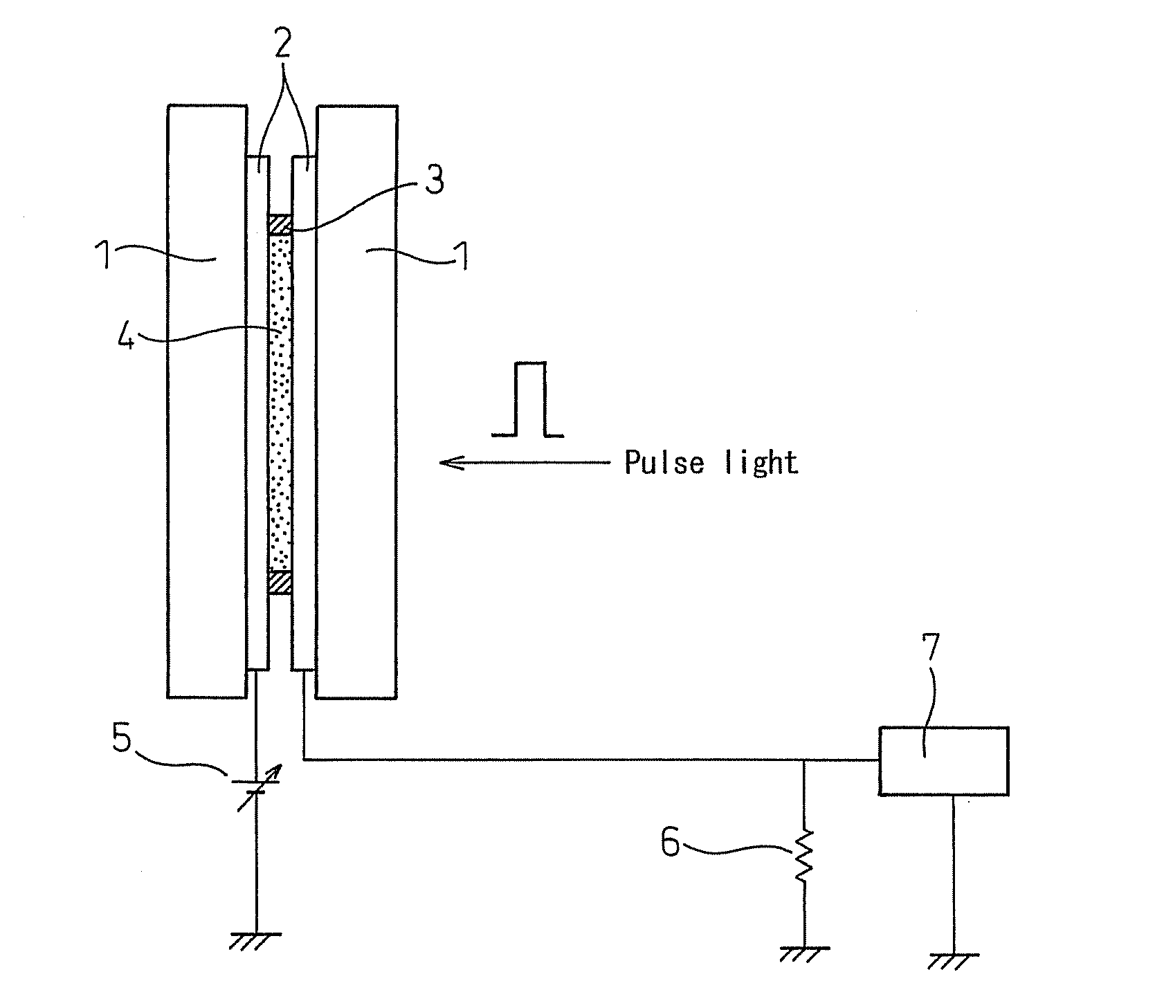
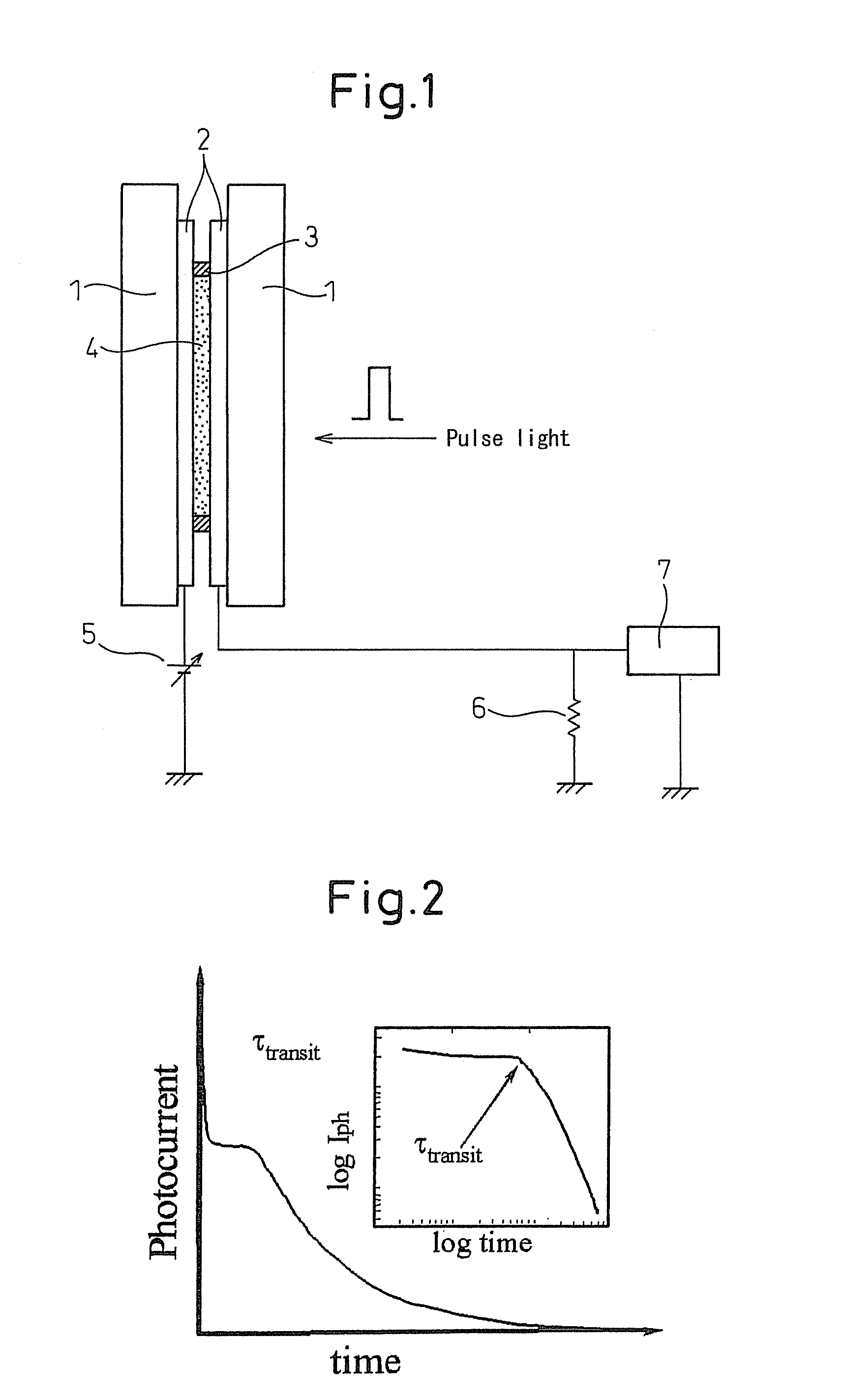
[0088]A purified TPD (N,N′-diphenyl-N,N′-bis(3-methylphenyl)-[1,1′-diphenyl]-4,4′-diamine) was injected into a liquid crystal cell at the temperature of the isotropic phase. The transient photocurrent was measured by the above time-of-flight method to determine a mobility of the material from the transit time of the charge. The mobilities of a positive charge and a negative charge obtained at a measurement temperature of 150° C. were 4×10⁻³ cm2 / Vs and 4×10⁻³ cm2 / Vs, respectively. From the mobilities, the conduction can be determined to be not the ionic conduction, but the electronic conduction caused by each of the hole and the electron.

[0089]In the same manner, in the purified TTA(tritolylamine), the mobilities of the positive charge and the negative charge at 100° C. were determined to be 4×10⁻³ cm2 / Vs and 9×10⁻⁵ cm2 / Vs, respecti...

example 2

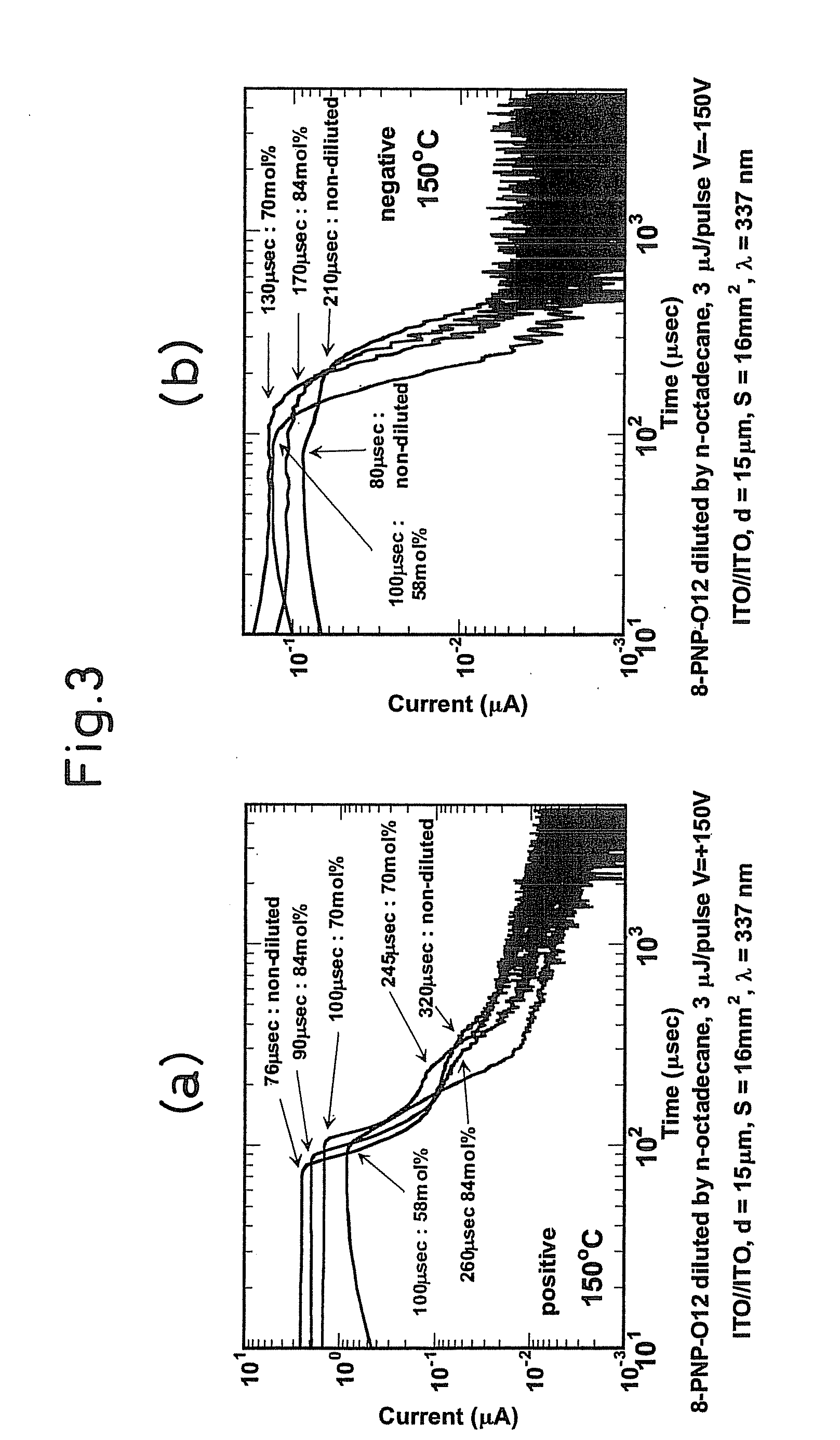
[0091]A 6-(4′-octylphenyl)-2-dodecyloxynaphtalene(8-PNP-012) was injected in an isotropic phase (liquid phase: in a thickness of the sample of 15 μm.) into a glass cell having an ITO electrode (4 mm square) positioned therein. A 337 nm nitrogen laser pulsed light (pulse width: 600 ps, 3 μJ / pulse) was radiated to apply voltages of +150 V or −150 V to the electrode on the light irradiation side, so that the transient photocurrent observed was measured by a digital oscilloscope. The wave profiles (in black) shown in FIG. 5 (whose left side illustrated the waveform of a transient photocurrent of the positive charge, and whose right side illustrated the waveform of a transient photocurrent of the negative charge) had two shoulders corresponding to transit times in different time regions. In order to clarify the conduction, the dilution experiment using an n-octadecane was performed. When the concentration of the n-octadecane was changed from 16 mol % to 42 mol %, the change of waveform o...

example 3

[0094]A 2-phenylnaphthalene in an isotropic phase (liquid phase: in a thickness of the sample of 16.31 μm) was charged into a glass cell having an ITO electrode (4 mm square) positioned therein in the same manner as in Example 2. A 337 nm nitrogen laser pulsed light (pulse width: 600 ps, 3 μJ / pulse) was radiated at 105° C. to apply voltages of +10 to 100 V or −10 to 100 V to the electrode on the light irradiation side, so that the transient photocurrent was observed and measured by a digital oscilloscope. The waveform of the transient photocurrent was shown in FIG. 5. The waveform of the positive charge has one stepped part representing a charge travelling in an early time region. The waveform of the negative charge has “two shoulders” corresponding to two different travelling time regions.

[0095]In the same manner as in Example 2, According to the result of the dilution experiment, the mobilities of the hole and electron were determined to be 8.9×10⁻⁴ cm2 / Vs, and 8.8×10⁻⁴ cm2 / Vs, re...


PUM


Abstract

An organic material having at least one aromatic conjugated π-electron system is selected. The purity of the organic material is improved by purification, and a conduction mechanism of the organic material is confirmed by a time-of-flight method, whereby a liquid phase of the organic material is usable as an organic semiconductor. A method that enables the usage of a liquid phase of an organic material as an organic semiconductor is provided. The method involves confirming the electronic conduction of the organic material having at least one aromatic conjugated π-electron system by evaluation of a charge transport property using a time-of-flight method, and by evaluation of a dilution effect caused by addition of a diluent.

Description

TECHNICAL FIELD[0001]The present invention relates to an organic material capable of exhibiting an electronic conduction. The liquid organic semiconductor material according to the present invention can be applied to various wide fields, and can achieve a new process for producing an organic electronic device, or a new form thereof. Specific examples of such an organic electronic device may include: optical sensor, organic EL (electro-luminescence) device, organic transistor, organic solar cell, or organic semiconductor memory.BACKGROUND ART[0002]An organic semiconductor material is a material which can be used for an optical sensor, an organic photoreceptor, an organic EL element, an organic transistor, an organic solar cell, an organic semiconductor memory, and the like. Specific examples of the organic semiconductor material which have heretofore been used may include: for example, an amorphous thin film or polycrystalline thin film which has been formed on a by using vacuum depo...

Claims


Application Information

Patent Timeline
IPC IPC(8): H01L51/30
CPCH01L51/0052H01L51/42Y02E10/549H01L51/5048H01L51/5012H10K85/615H10K50/14H10K50/11H10K85/111H10K30/00
Inventor HANNA, JUN-ICHITOKUNAGA, KEIJIIINO, HIROAKI
Owner JAPAN SCI & TECH CORP
Learn More