Semiconductor device and manufacturing method thereof

a technology of semiconductor devices and manufacturing methods, applied in semiconductor devices, electrical devices, transistors, etc., can solve the problems of not being able to be formed over a larger glass substrate, and achieve the effect of low power consumption and small off-state curren

Inactive Publication Date: 2012-07-12
SEMICON ENERGY LAB CO LTD
View PDF4 Cites 58 Cited by
  • Summary
  • Abstract
  • Description
  • Claims
  • Application Information

AI Technical Summary

Benefits of technology

[0024]Oxygen deficiency in the oxide semiconductor serves as a donor and generates a carrier. That is, oxygen deficiency makes the side surface of the oxide semiconductor layer n-type, which causes unintended current (leakage current) in the side surface of the oxide semiconductor layer. Current which flows in the side surface of the oxide semiconductor layer increases the off-state current of the transistor.
[0025]The side surface of the oxide semiconductor layer is covered with an insulating layer containing oxygen, so that current flowing at the side surface of the oxide semiconductor layer can be reduced.
[0026]Since current easily flows in the side surface of the oxide semiconductor layer, preferably...

Problems solved by technology

On the other hand, although a transistor manufactured using polycrystalline silicon has ...

Method used


Image

  • Semiconductor device and manufacturing method thereof
  • Semiconductor device and manufacturing method thereof
  • Semiconductor device and manufacturing method thereof

Examples


embodiment 1

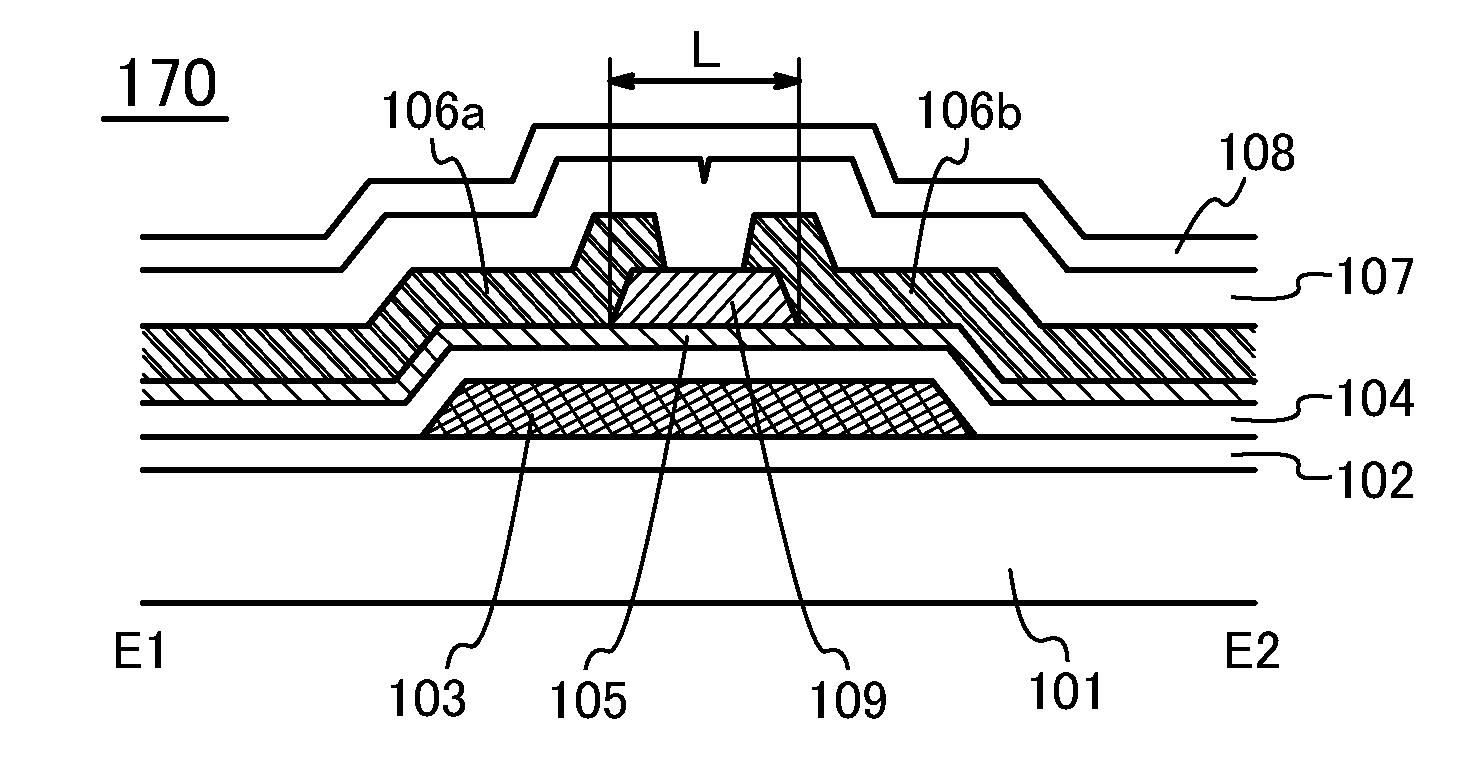
[0060]In this embodiment, a transistor in which an oxide semiconductor is used for a semiconductor layer where a channel is formed and a manufacturing method thereof will be described with reference to FIGS. 1A to 1C, FIGS. 2A to 2C, FIGS. 3A to 3C, FIGS. 4A to 4C, FIGS. 5A to 5C, FIGS. 6A to 6C, FIGS. 7A to 7C, and FIGS. 8A and 8B.

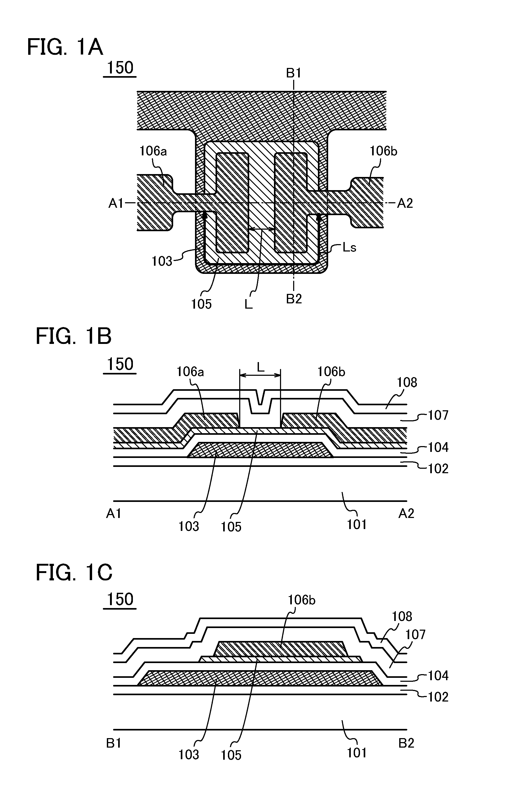
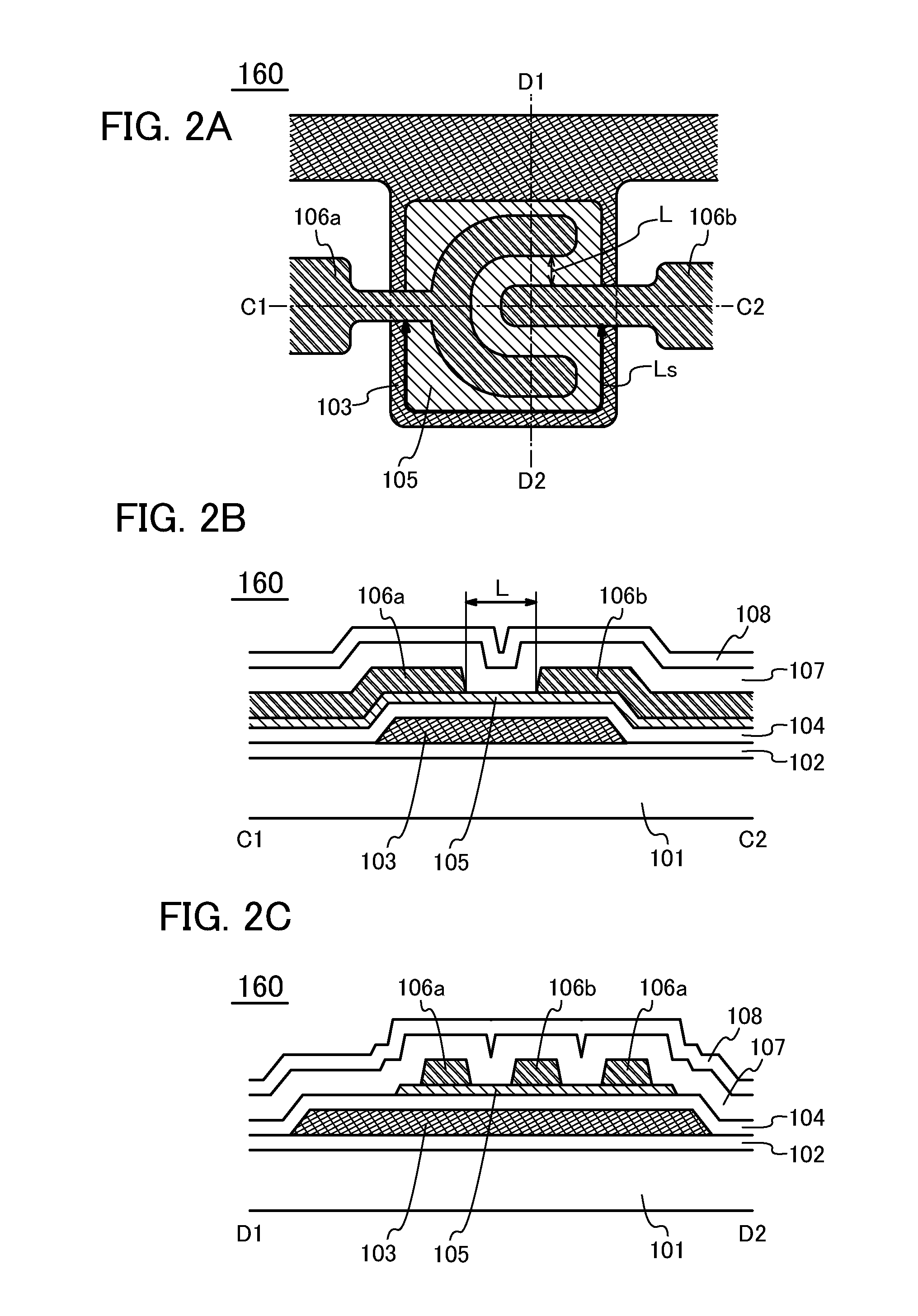
[0061]FIG. 1A is a top-view illustrating a structure of a transistor 150 which is one embodiment of a semiconductor device. FIG. 1B is a cross-sectional view illustrating a stacked-layer structure of a portion taken along the chain line A1-A2 in FIG. 1A. FIG. 1C is a cross-sectional view illustrating a stacked-layer structure of a portion taken along the chain line B1-B2 in FIG. 1A. Note that the description of a substrate and an insulating layer are omitted in FIG. 1A.

[0062]The transistor 150 in FIGS. 1A to 1C includes a base layer 102 formed over a substrate 101 and a gate electrode 103 formed over the base layer 102. The transistor 150 further includes...

embodiment 2

[0178]In this embodiment, an example of a process which is partly different from that described in Embodiment 1 will be described with reference to FIGS. 9A to 9C. Note that the same reference numerals are used for the same parts as those in Embodiment 1, and specific description of the parts with the same reference numerals is omitted here.

[0179]First, as in Embodiment 1, the base layer 102 is formed over the substrate 101, and the gate electrode 103 is formed over the base layer 102.

[0180]Then, the gate insulating layer 104 is formed over the gate electrode 103, and a first oxide semiconductor layer with a thickness of 1 nm to 10 nm is formed over the gate insulating layer 104. In this embodiment, the first oxide semiconductor layer is formed to a thickness of 5 nm by using a sputtering gas of oxygen under such conditions that a target for an oxide semiconductor (a target for an In—Ga—Zn-based oxide semiconductor (In2O3: Ga2O3: ZnO=1:1:2 [molar ratio]) is used, the distance betwee...

embodiment 3

[0191]In this embodiment, a method for forming an oxide semiconductor including CAAC-OS, which is different from the method disclosed in Embodiment 2, will be described.

[0192]First, over the gate insulating layer 104, an oxide semiconductor is formed with a thickness of 1 nm to 50 nm.

[0193]The substrate temperature in the film formation is 150° C. to 450° C., preferably 200° C. to 350° C. The deposition is performed while the substrate is heated in the range of 150° C. to 450° C., preferably 200° C. to 350° C., whereby moisture (including hydrogen) or the like is prevented from entering a film. Further, CAAC-OS which is an oxide semiconductor including crystal can be formed.

[0194]Further, it is preferable that hydrogen be further released from the oxide semiconductor and oxygen contained in the gate insulating layer 104 be partly diffused into the oxide semiconductor and the vicinity of the interface of the oxide semiconductor in the gate insulating layer 104 by performing heat trea...


PUM


Abstract

The semiconductor device includes a gate electrode over a substrate, a gate insulating layer over the gate electrode, an oxide semiconductor layer over the gate insulating layer, and a source electrode and a drain electrode over the oxide semiconductor layer. A length of part of an outer edge of the oxide semiconductor layer from an outer edge of the source electrode to an outer edge of the drain electrode is more than three times, preferably more than five times as long as a channel length of the semiconductor device. Further, oxygen is supplied from the gate insulating layer to the oxide semiconductor layer by heat treatment. In addition, an insulating layer is formed after the oxide semiconductor layer is selectively etched.

Description

BACKGROUND OF THE INVENTION[0001]1. Field of the Invention[0002]The present invention relates to a semiconductor device which includes a circuit including a semiconductor element such as a transistor, and a manufacturing method of the semiconductor device. For example, the present invention relates to a power device which is mounted on a power supply circuit; a semiconductor integrated circuit including a memory, a thyristor, a converter, an image sensor, or the like; and an electronic device on which an electro-optical device typified by a liquid crystal display panel, a light-emitting display device including a light-emitting element, or the like is mounted as a component.[0003]In this specification, a semiconductor device generally refers to a device which can function by utilizing semiconductor characteristics; an electro-optical device, a light-emitting display device, a semiconductor circuit, and an electronic device are all included in the category of the semiconductor device...

Claims


Application Information

Patent Timeline
IPC IPC(8): H01L29/786H01L21/34
CPCH01L21/02554H01L21/02565H01L21/02631H01L29/7869H01L29/66969H01L21/467H01L21/469H01L21/477H01L29/78693H01L29/66742H01L29/78618H01L27/1288H01L27/127H01L27/1259H01L27/1214
Inventor YAMAZAKI, SHUNPEI
Owner SEMICON ENERGY LAB CO LTD
Why Eureka
Try Eureka