

Semiconductor device and manufacturing method thereof
a semiconductor film and semiconductor technology, applied in the direction of transistors, electroluminescent light sources, electric lighting sources, etc., can solve the problems of high leakage current between a source and a drain of the transistor, oxygen defect, oxygen vacancy or oxygen deficiency, etc., to reduce the negative shift of the threshold voltage of the transistor, reduce the oxygen defect in the oxide semiconductor film, and reduce the effect of leakage curren
- Summary
- Abstract
- Description
- Claims
- Application Information
AI Technical Summary
Benefits of technology
Problems solved by technology
Method used
Image

Examples
embodiment 1
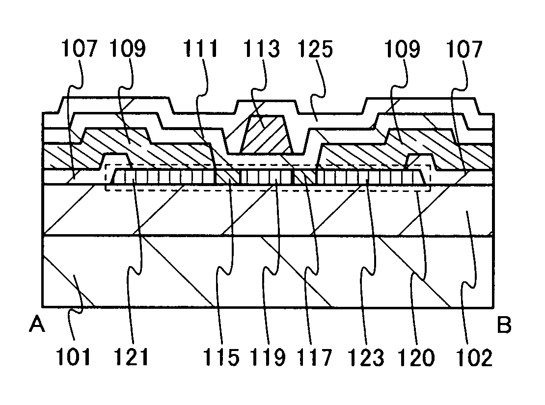
[0059]In this embodiment, a structure of a transistor in which a leakage current can be reduced and a manufacturing method of the transistor will be described with reference to FIGS. 1A to 1D, FIGS. 2A to 2E, and FIGS. 3A to 3C.
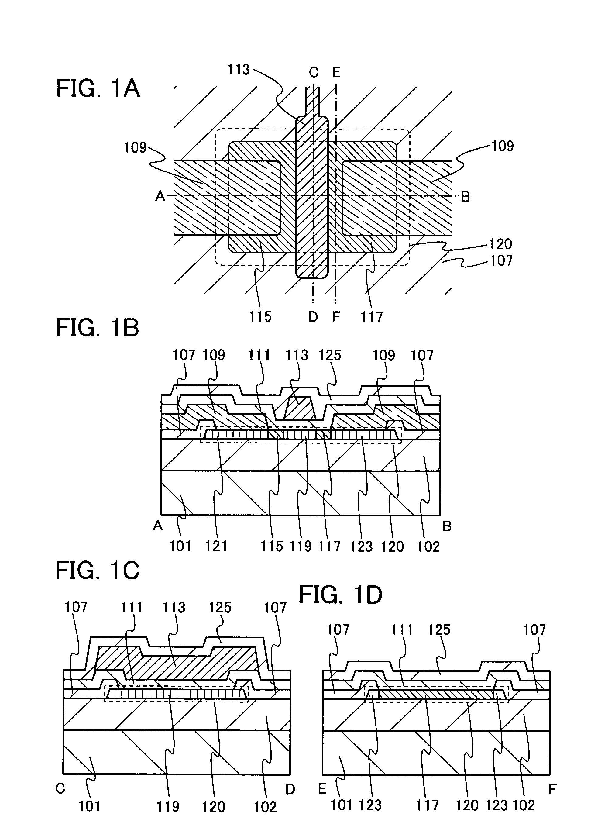
[0060]FIGS. 1A to 1D are a top view and cross-sectional views of a transistor described in this embodiment. FIG. 1A is the top view of the transistor described in this embodiment, FIG. 1B is a cross-sectional view taken along a dashed-dotted line A-B in FIG. 1A, FIG. 1C is a cross-sectional view taken along a dashed-dotted line C-D in FIG. 1A, and FIG. 1D is a cross-sectional view taken along a dashed-dotted line E-F in FIG. 1A. In FIG. 1A, some of components of the transistor (e.g., a gate insulating film 111, an insulating film 125, and the like) are not shown for simplicity.
[0061]The transistor illustrated in FIGS. 1A to 1D includes an oxide insulating film 102 provided over a substrate 101, an oxide semiconductor film 120 provided over the oxide insulatin...
embodiment 2
[0161]In this embodiment, a method for manufacturing the transistor of FIGS. 1A to 1D, which is different from that described in Embodiment 1, will be described with reference to FIGS. 3A to 3C and FIGS. 4A to 4D.
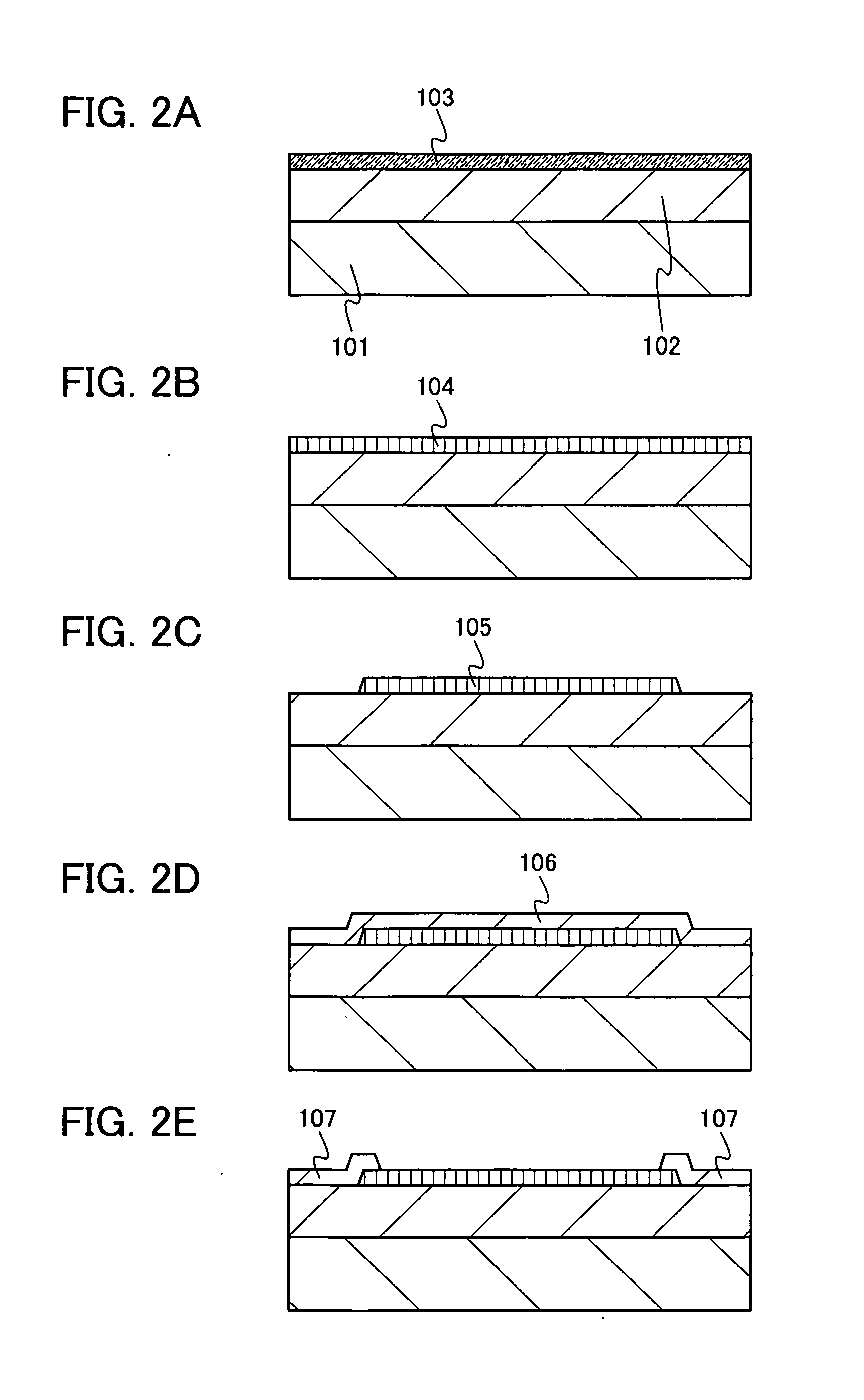
[0162]In a manner similar to that of Embodiment 1, the oxide insulating film 102 is formed over the substrate 101 as illustrated in FIG. 4A. Next, the oxide semiconductor film 103 is formed over the oxide insulating film 102. It is preferable that the oxide insulating film 102 and the oxide semiconductor film 103 be formed successively. A multi-chamber sputtering apparatus having a heating apparatus may be employed in the following manner: the oxide insulating film 102 is formed and heated with the heating apparatus so that hydrogen is released, and then the oxide semiconductor film 103 is formed over the oxide insulating film 102.
[0163]Then, a mask is formed over the oxide semiconductor film 103, and the oxide semiconductor film 103 is selectively etched with the use of th...
embodiment 3
[0169]In this embodiment, a method for manufacturing a transistor, which is different from those described in Embodiment 1 and Embodiment 2, will be described with reference to FIGS. 3A to 3C, FIGS. 5A to 5C, and FIG. 6. This embodiment will be described as another embodiment of the method for manufacturing a transistor in Embodiment 1; however, Embodiment 2 can be applied to this embodiment as appropriate. FIG. 6 is a top view illustrating a formation step of an insulating film 145, and FIG. 5A is a cross-sectional view taken along a dashed-dotted line A-B in FIG. 6.
[0170]In a manner similar to that of Embodiment 1, after the process of FIGS. 2A to 2D, as illustrated in FIG. 5A and FIG. 6, an insulating film 145 having an opening 141 and an opening 143 is formed. Next, as illustrated in FIG. 5B, a conductive film 147 is formed over the oxide semiconductor film 105 and the insulating film 145. The conductive film 147 can be formed as appropriate using a material and a formation meth...
PUM
 Abstract
Description
Claims
Application Information