Combined-source Mos Transistor with Comb-shaped Gate, and Method for Manufacturing the Same

a technology of mos transistor and comb gate, which is applied in the field of combined-source mos transistor, can solve the problems of constant rise of subthreshold leakage current, inability to reduce the subthreshold slope of the conventional mosfet device, and increase the power consumption of the integrated circuit, so as to improve the performance of the device, improve the manufacturing method, and increase the turn-on current

Active Publication Date: 2012-07-19
SEMICON MFG INT (SHANGHAI) CORP +1
View PDF1 Cites 3 Cited by
  • Summary
  • Abstract
  • Description
  • Claims
  • Application Information

AI Technical Summary

Benefits of technology

[0029]Briefly, the device according to embodiments of the present invention employs a combined-source structure and includes a Schottky Barrier and a comb-shaped gate structure, thereby a performance of the device is improved and a manufacturing method is simple. As compared with an existing MOSFET, under the same

Problems solved by technology

A Drain-Induced Barrier lowering (DIBL) effect and a band-to-band tunneling effect make an off-state leakage current of the device larger and larger, and as a threshold voltage of the device lowers, a power consumption of the integrated circuit increases.
Moreover, due to theoretically limited by KT/q, a subthreshold slope of the conventional MOSFET device cannot decrease as the device size reduces simultaneously, and a subthreshold leakage current r

Method used


Image

  • Combined-source Mos Transistor with Comb-shaped Gate, and Method for Manufacturing the Same
  • Combined-source Mos Transistor with Comb-shaped Gate, and Method for Manufacturing the Same
  • Combined-source Mos Transistor with Comb-shaped Gate, and Method for Manufacturing the Same

Examples


Embodiment Construction

[0046]Further illustration will now be given on the invention by examples. It should be noted that the object of the embodiments disclosed is to help to further understand the invention. However, one skilled in the art may appreciate that various substitutions and modifications can be made without departing from the spirit and scope of the invention and the appended claims. Therefore, the invention should not be limited to the embodiments disclosed; instead, the scope of the invention will be defined by the appended claims and their equivalents.

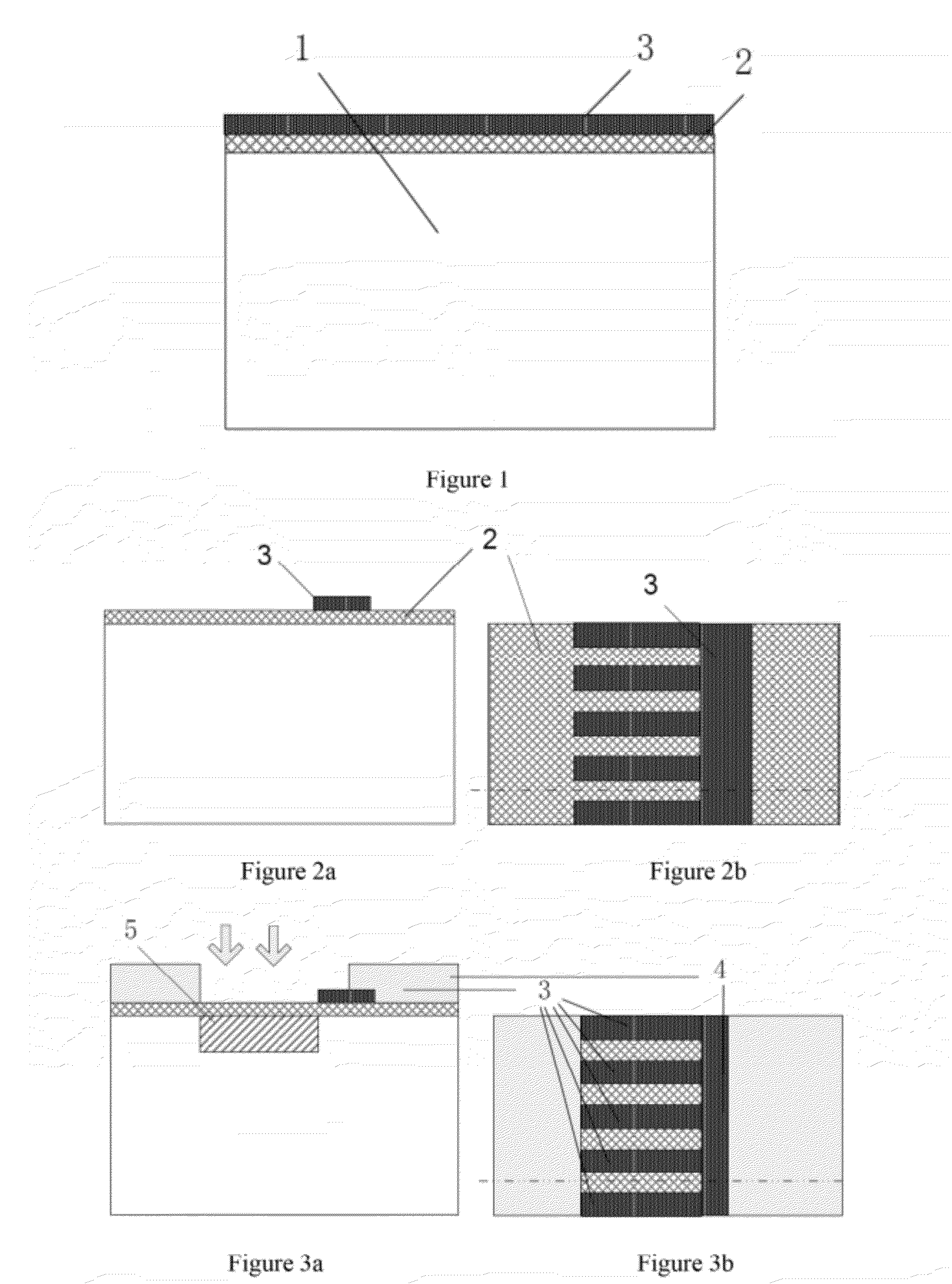
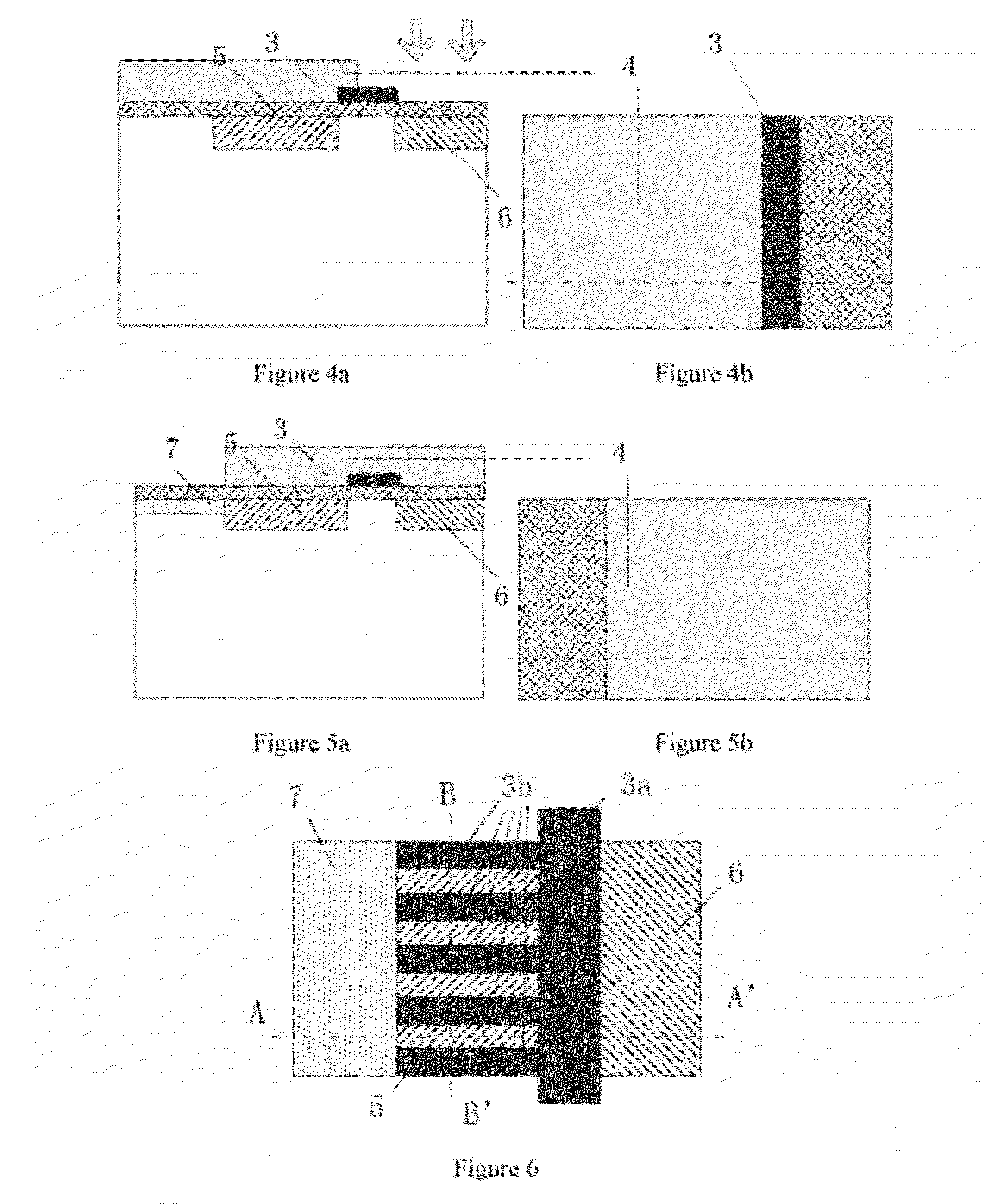
[0047]One embodiment of a manufacturing method according to the invention comprises process steps as shown in FIG. 1 to FIG. 5b.

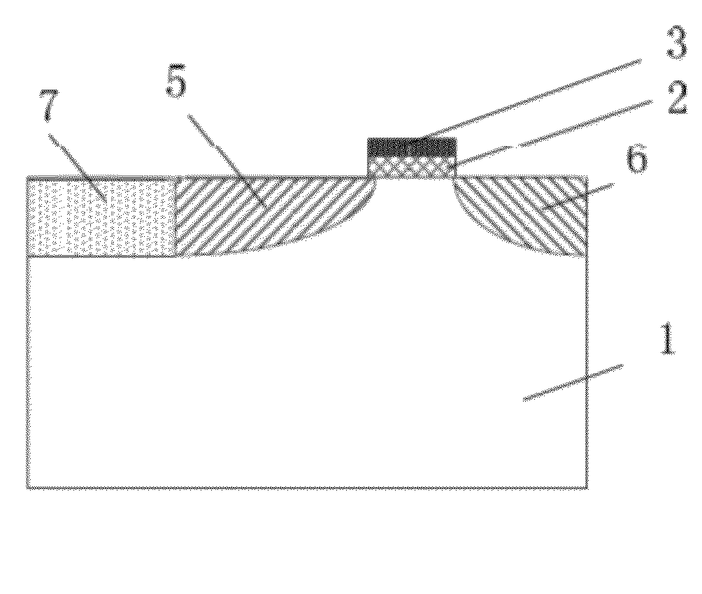
[0048]1. An isolation layer of an active region is formed on a bulk silicon substrate 1 with a crystal orientation of (100) via a shallow trench isolation technology, and a doping concentration of the substrate is a light doping. Then, a gate dielectric layer 2 is formed by a thermal growth, and the gate dielectric ...


PUM


Abstract

The present invention discloses a combined-source MOS transistor with a Schottky Barrier and a comb-shaped gate structure, and a method for manufacturing the same. The combined-source MOS transistor includes: a control gate electrode layer, a gate dielectric layer, a semiconductor substrate, a highly-doped source region and a highly-doped drain region, wherein a Schottky source region is connected to a side of the highly-doped source region which is far from a channel, one end of the control gate extends to the highly-doped source region, the extended gate region is an extension gate in a form of a comb-shaped and the original control gate region is a main gate; an active region covered by the extension gate is also a channel region, and is a substrate material; the highly-doped source region which is formed by highly doping is located on both sides of each comb finger of the extension gate; and a Schottky junction is formed at a location where the Schottky source region and the channel under the extension gate are located. As compared with an existing MOSFET, in the invention, a higher turn-on current, a lower leakage current and a steeper subthreshold slope may be obtained under the same process condition and the same active region size.

Description

FIELD OF THE INVENTION[0001]The present invention relates to a field of Field-Effect-Transistor (FET) logic devices and circuits in CMOS ultra-large-scale integrated (ULSI) circuits, and in particular, to a combined-source MOS transistor with a Schottky Barrier and a comb-shaped gate structure, and a method for manufacturing the same.BACKGROUND OF THE INVENTION[0002]As a size of a Metal-Oxide-Silicon Field Effect Transistor (MOSFET) becomes smaller and smaller, especially when a feature size of the device enters a nanometer scale, a negative influence of a short-channel effect of the device also becomes more and more apparent. A Drain-Induced Barrier lowering (DIBL) effect and a band-to-band tunneling effect make an off-state leakage current of the device larger and larger, and as a threshold voltage of the device lowers, a power consumption of the integrated circuit increases. Moreover, due to theoretically limited by KT / q, a subthreshold slope of the conventional MOSFET device can...

Claims


Application Information

Patent Timeline
IPC IPC(8): H01L29/78H01L21/336
CPCH01L29/4238H01L29/7839H01L29/7391H01L29/66643
Inventor HUANG, RUHUANG, QIANQIANZHAN, ZHANWANG, YANGYUAN
Owner SEMICON MFG INT (SHANGHAI) CORP
Why Eureka
Try Eureka