Bumped semiconductor wafer or die level electrical interconnect

a semiconductor wafer or die level, electrical interconnection technology, applied in the direction of electronic circuit testing, measurement devices, instruments, etc., can solve the problems of reducing the electrical performance of the connection, affecting the self-heating effect of the contact, and the probe is usually more expensive, so as to achieve the effect of improving the electrical performan

Inactive Publication Date: 2012-07-19
HSIO TECH
View PDF2 Cites 59 Cited by
  • Summary
  • Abstract
  • Description
  • Claims
  • Application Information

AI Technical Summary

Benefits of technology

[0029]The use of additive printing processes can permit the material set in a given layer of a probe assembly to vary. Traditional PCB and circuit fabrication methods take sheets of material and stack them up, laminate, and/or drill. Additive printing technologies permit a wide variety of materials to be applied on a layer with a registration relative to the features of the previous layer. Selective addition of conductive, non-conductive, or semi-conductive materials at precise locations to create a desired effect has the major advantages in tuning i

Problems solved by technology

Long contact members, however, tend to reduce the electrical performance of the connection by creating a parasitic effect that impacts the signal as it travels through the contact.
Resistance in the contacts impacts the self heating effects as current passes through power delivery contacts.
Also, the small space between contacts can cause distortion known as cross talk as a nearby contact may influence its neighbor.
In most cases, the tests that are run using needle probes are typically basic on-off tests due to the limited signal integrity.
These probes are usually more expensive, and are typically used for area array connections.
Again, the length of the contact wire to allow the beam to buckle is relatively large, so the signal performance can be impacted.
Micro spring and MEMS-based probes are typically very expensive, and although better electrically than the longer probe styles, they may have electrical limitations.
Membrane probes typically have the be

Method used


Image

  • Bumped semiconductor wafer or die level electrical interconnect
  • Bumped semiconductor wafer or die level electrical interconnect
  • Bumped semiconductor wafer or die level electrical interconnect

Examples


Embodiment Construction

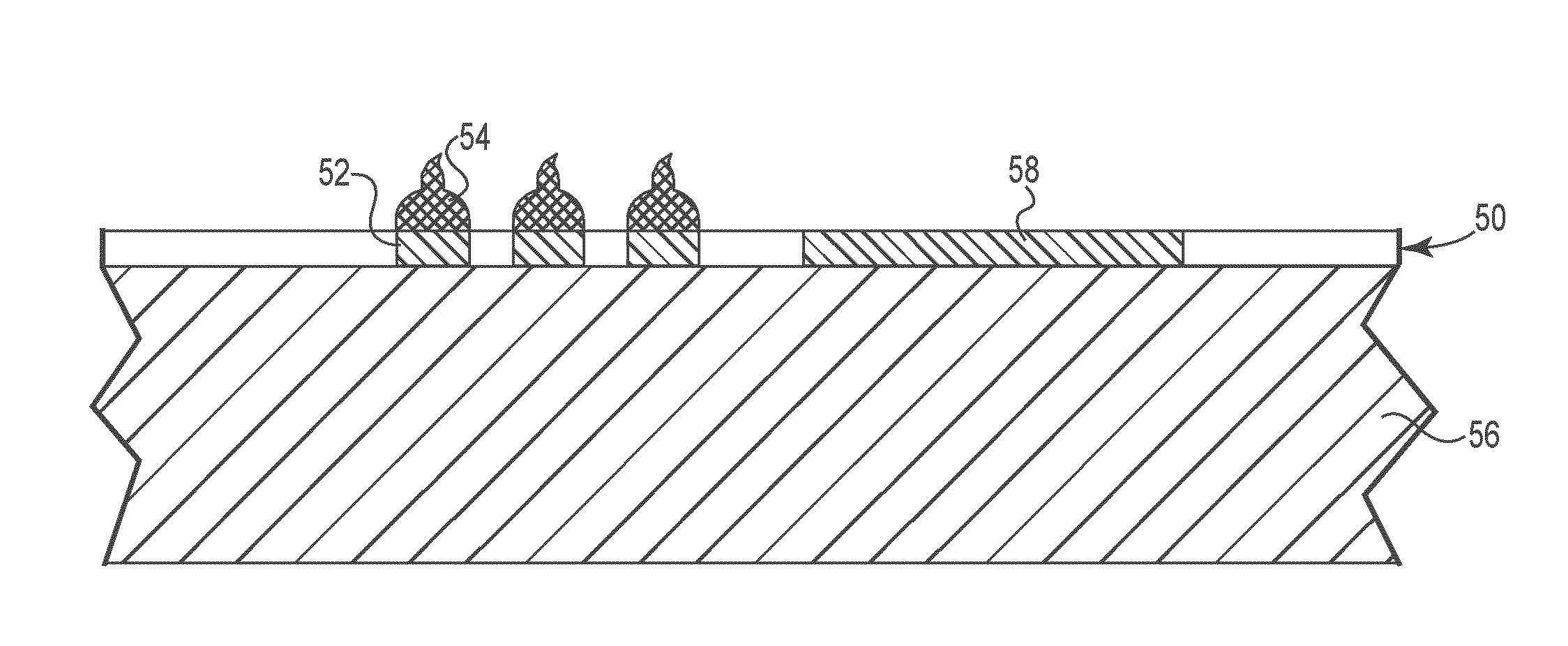
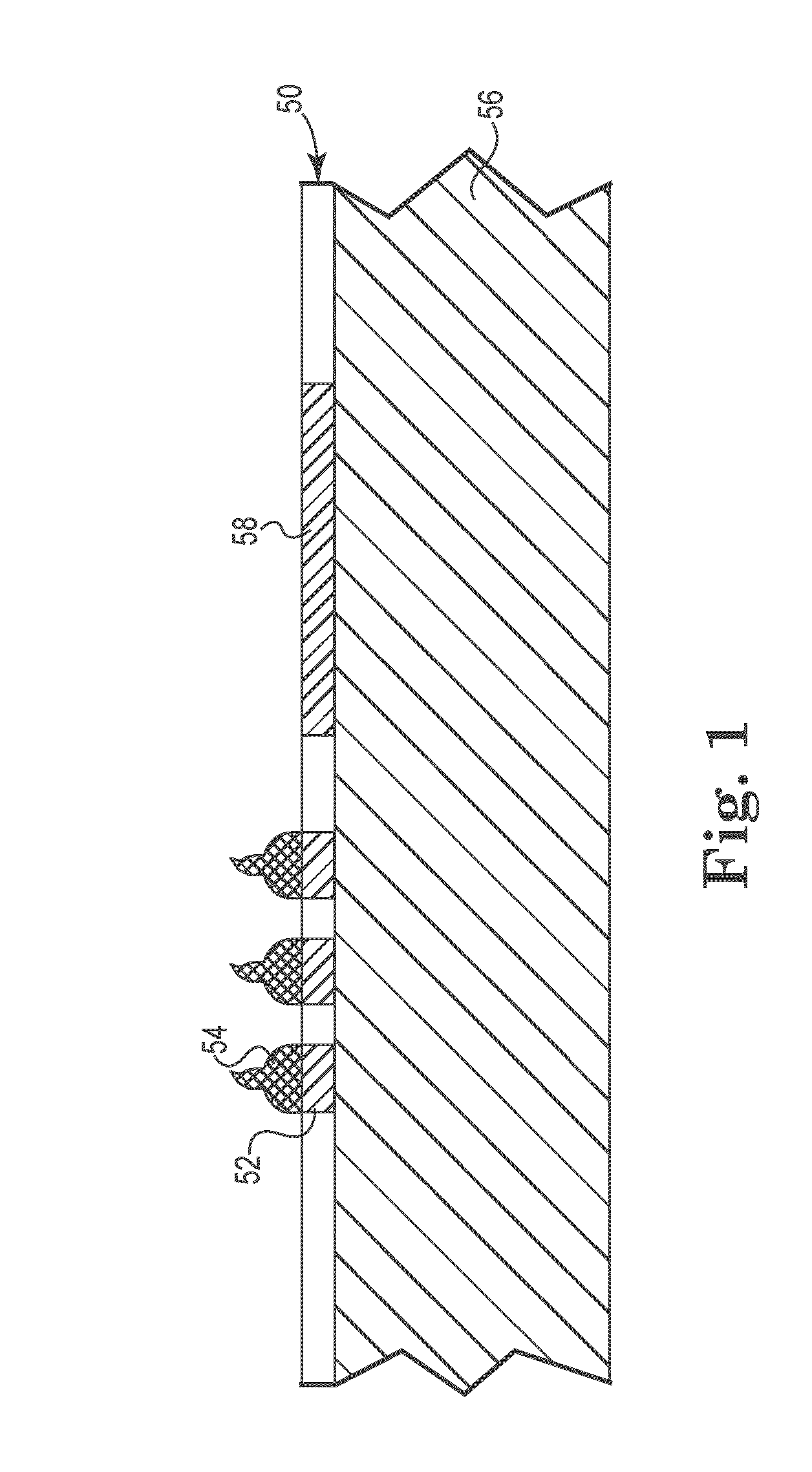
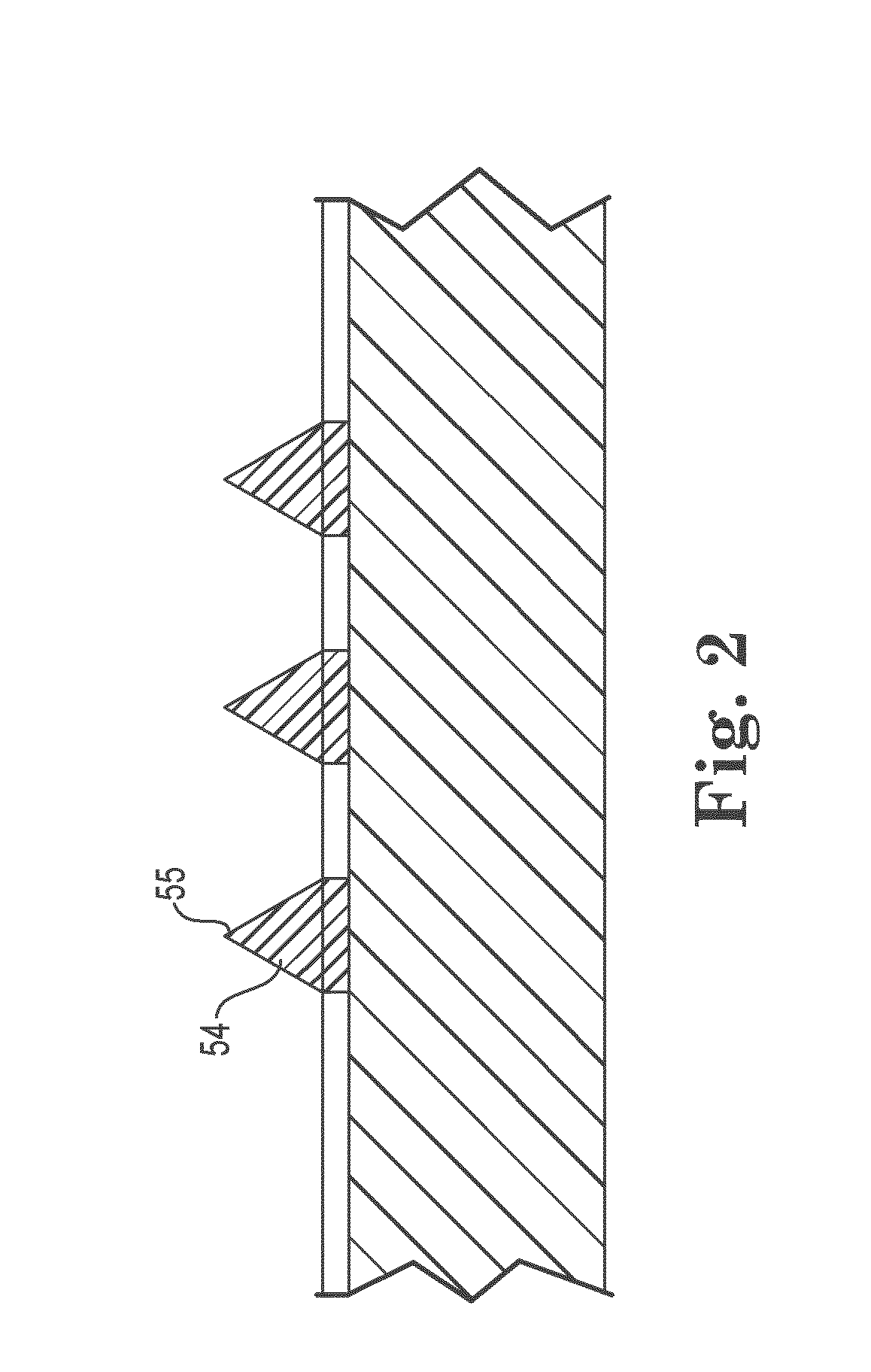
[0052]The present disclosure relates to a high performance probe assembly for testing wafer-level integrated circuits. The present probe assembly can be used with electrical devices having contact-to-contact spacing (pitch) on the order of less than about 1.0 millimeter (1×10⁻³ meters), and more preferably a pitch of less than about 0.7 millimeter, and most preferably a pitch of less than about 0.4 millimeter. Such fine pitch probe assemblies are especially useful for probing wafer-level integrated circuits.

[0053]FIG. 1 illustrates a probe assembly 50 that leverages the principle of stud bumping in accordance with an embodiment of the present disclosure. Stud bumping is a derivation of wire bonding, both of which have been used for many years in the semiconductor packaging industry. In recent years, the cost of gold has driven a migration to the use of copper bonding wire in an effort to reduce cost.

[0054]Substrate 56 is positioned appropriately within the bond area and stud bumps 5...


PUM


Abstract

A probe assembly that acts as a temporary interconnect between terminals on an IC device and a test station. The probe assembly includes a plurality of stud bumps arranged on a first surface of a substrate in a configuration corresponding to the terminal on the IC device. The stud bumps include a shape adapted to temporarily couple with the terminals on the IC device. A plurality of conductive traces on the substrate electrically couple the stud bumps with the test station.

Description

RELATED APPLICATIONS[0001]The present application claims the benefit of U.S. Provisional Application No. 61 / 449,871, entitled Bumped Semiconductor Wafer or Die Level Electrical Interconnect, filed Mar. 7, 2011.[0002]This application is continuation-in-part of U.S. patent application Ser. No. 13 / 266,522, titled COMPLIANT WAFER LEVEL PROBE ASSEMBLY, filed Oct. 27, 2011, which is a national stage application under 35 U.S.C. §371 of International Application No. PCT / US2010 / 036047, titled COMPLIANT WAFER LEVEL PROBE ASSEMBLY, filed May 25, 2010, which claims priority to U.S. Provisional Application No. 61 / 183,856, filed Jun. 3, 2009, both of which are hereby incorporated by reference in their entireties.[0003]This application is a continuation-in-part of U.S. patent application Ser. No. 13 / 266,573, titled COMPLIANT PRINTED CIRCUIT AREA ARRAY SEMICONDUCTOR DEVICE PACKAGE, filed Oct. 27, 2011, which is a national stage application under 35 U.S.C. §371 of International Application No. PCT / U...

Claims


Application Information

Patent Timeline
IPC IPC(8): G01R31/20
CPCG01R31/2889
Inventor RATHBURN, JAMES
Owner HSIO TECH
Why Eureka
Try Eureka