

Pellicle film and a pellicle for EUV application, and a method for manufacturing the film
a technology of pellicle and euv, which is applied in the field of pellicle for euv (extreme ultra violet) lithography application, can solve the problems of resist, pellicle, and large obstacle to the realization of euv exposure lithography, and achieves good yield ratio, excellent transmittance, and sufficient strength
- Summary
- Abstract
- Description
- Claims
- Application Information
AI Technical Summary
Benefits of technology
Problems solved by technology
Method used
Image


Examples
example 1
[0033]As the starting plate, an SOI (Silicon On Insulator) plate consisting of successively a handle plate of 200 mm diameter and 725 μm thickness, a 150 nm thick thermally grown silicon oxide (SiO2) layer and a 100 nm thick thin layer of silicon single crystal (Nearly Perfect Crystal: NPC) was used. The handle plate is a silicon plate and the silicon single crystal does not substantially contain any crystal defects such as COP (Crystal Originated Particle: void defect).
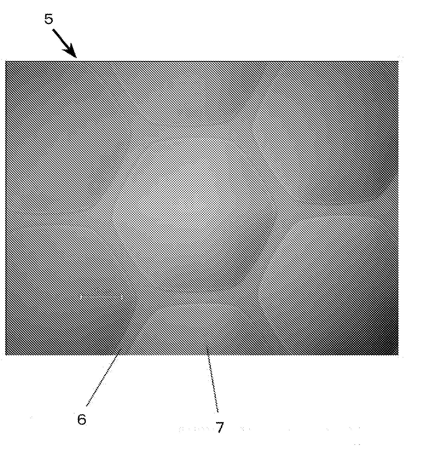
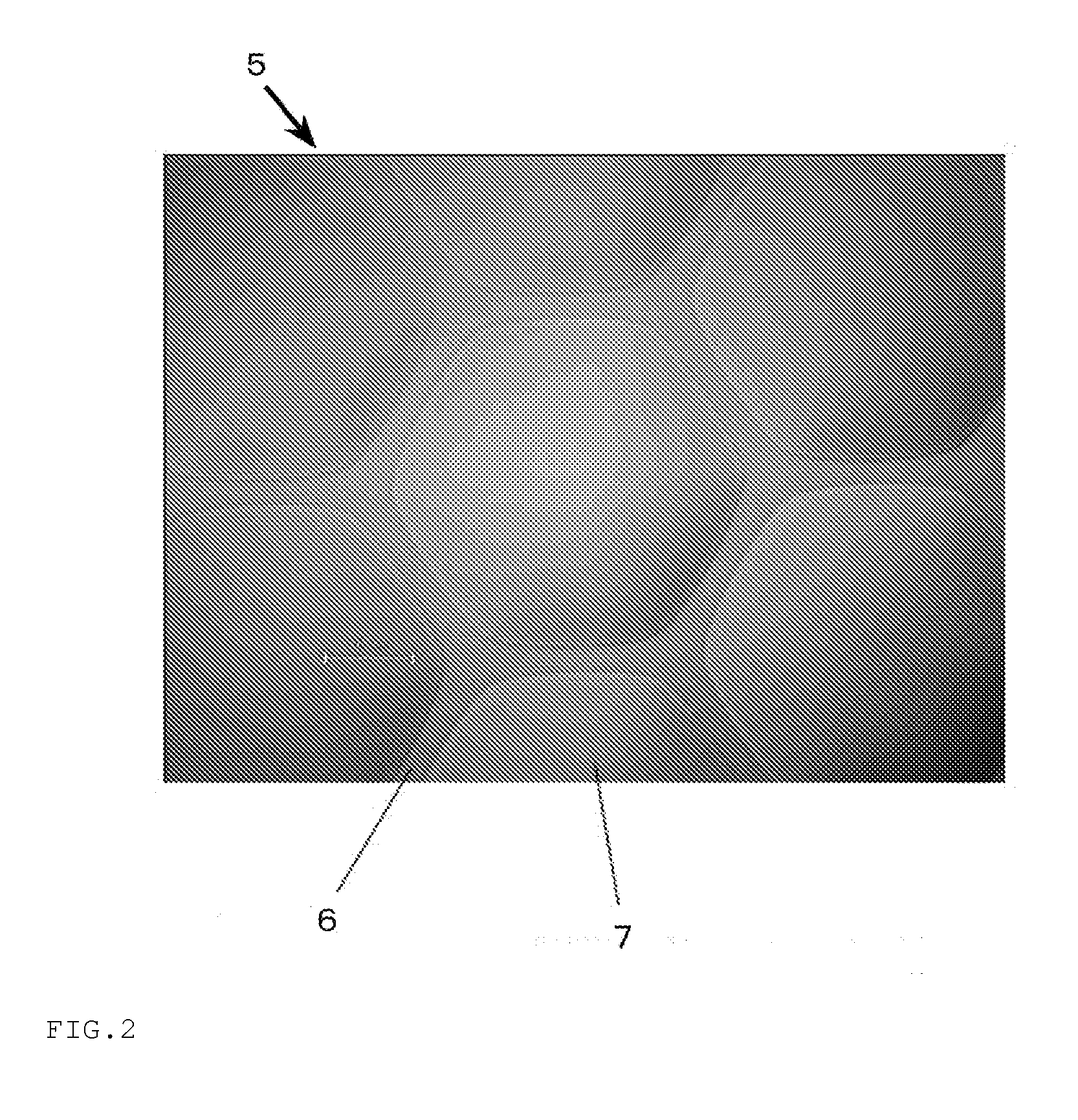
[0034]First, the handle plate portion of the SOI plate was thinned to 300 μm; next, the handle plate was patterned to have a mesh pattern 4 by lithography, then dry-etching was carried out to have a mesh structure. After that, the exposed portions of the BOX layer (silicon oxide layer) were removed by using HF to complete a pellicle film (see FIG. 1).
example 2
[0035]As the starting plate, an SOI (Silicon On Insulator) plate consisting of successively a handle plate of 200 mm diameter and 725 μm thickness, a 10 nm thick thermally grown silicon oxide (SiO2) layer and a 100 nm thick thin layer of silicon single crystal (Nearly Perfect Crystal: NPC) was used. The handle plate is a silicon plate and the silicon single crystal does not substantially contain any crystal defects such as COP.
[0036]The aforementioned handle plate portion of the SOI plate was thinned to 30 μm. The handle plate was patterned to have a mesh pattern by lithography, then, dry-etching was carried out to have a mesh structure. After that, the exposed portions of the BOX oxide layer were removed by using HF to complete a pellicle film.
example 3
[0037]As the starting plate, an SOI (Silicon On Insulator) plate consisting of successively a handle plate of 200 mm diameter and 725 μm thickness, a 1 μm thick thermally grown silicon oxide (SiO2) layer and a 100 nm thick thin layer of silicon single crystal (Nearly Perfect Crystal) was used. The handle plate is a silicon plate and the single crystal silicon does not substantially contain any crystal defects such as COP.
[0038]The handle plate was patterned to have a mesh pattern by lithography, then, dry-etching was carried out to have a mesh structure. After that, the exposed portions of the BOX oxide layer were removed by using HF to complete a pellicle film.
PUM
 Abstract
Description
Claims
Application Information