

Semiconductor composition
- Summary
- Abstract
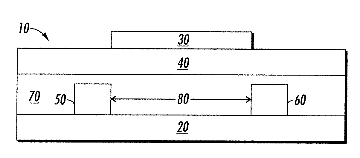
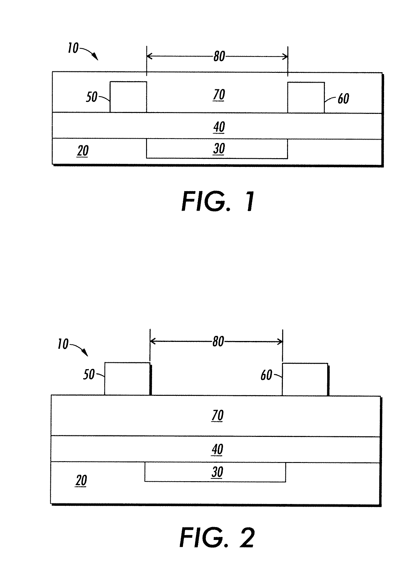
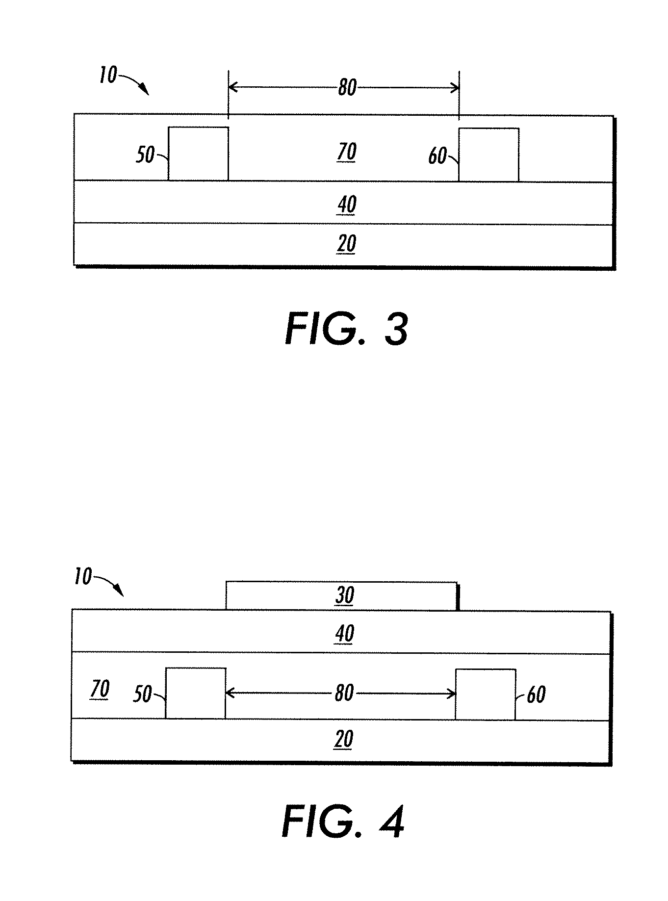
- Description
- Claims
- Application Information
AI Technical Summary
Benefits of technology
Problems solved by technology
Method used
Image

Examples
example 1
[0095]Single wall carbon nanotubes (Bucky USA, BU-203) were added to 1,2-dichlorobenzene until a concentration of 0.1 wt % carbon nanotubes was reached. The mixture was probe ultra-sonicated at 50% power for 20 seconds at room temperature to form a dispersion. PQT-12 powder was added to the carbon nanotube dispersion until a PQT-12 concentration of 0.1 wt % was obtained. At this point, the weight ratio of carbon nanotubes to PQT-12 was 1:1. The mixture was warmed to about 80 degree C. to dissolve the PQT-12 and then probe ultra-sonicated for 20 seconds in an ice-water bath (0-5 degree C.) to produce a very stable dispersion of carbon nanotubes and PQT-12 nanoparticles. The dispersion was centrifuged for 30 minutes, and no precipitation was observed. The PQT-12 is capable of forming nano-aggregates in 1,2-dichlorobenzene solvent. It is believed that the polymer aggregates help to stabilize the carbon nanotube dispersion. This composition is referred to as the PQT-12 stabilized CNT di...
example 2
[0099]Thin-film transistors were fabricated on a silicon wafer substrate using the CNT / PQT-12 composition of Example 1 to form a semiconducting layer. N-doped silicon functioned as the gate, and a 200 nm silicon oxide layer functioned as the dielectric layer. The silicon oxide was modified with octyltrichlorosilane. The CNT / PQT-12 composition was spin coated on the wafer at 1000 rpm for 120 seconds. The deposited semiconductor composition was dried at 80° C. and annealed at 140° C. in a vacuum oven to form the semiconducting layer. Gold source and drain electrodes were evaporated on top of the semiconductor through a shadow mask.
[0100]TFTs produced with the CNT / PQT-12 semiconducting layer showed a field
PUM
| Property | Measurement | Unit |
|---|---|---|
| Time | aaaaa | aaaaa |
| Temperature | aaaaa | aaaaa |
| Weight | aaaaa | aaaaa |
Abstract
Description
Claims
Application Information