Sensor chip for biomedical and micro-nano structured substances and method for manufacturing the same

a biomedical and micronano technology, applied in the direction of optical radiation measurement, instruments, spectrometry/spectrophotometry/monochromators, etc., can solve the problems of unstable signals, signal may be sometimes strong, and the activity of the sensor may be affected, so as to enhance the adhesion of specific bacteria, enhance the adhesion of analyte onto the sensor chip, and enhance the intensity of signals

Inactive Publication Date: 2012-08-02
NAT CHENG KUNG UNIV
View PDF14 Cites 21 Cited by
  • Summary
  • Abstract
  • Description
  • Claims
  • Application Information

AI Technical Summary

Benefits of technology

[0014]In the sensor chip of the present invention, the thickness of the barrier layer covering the second end of the anodized aluminum oxide film can range from 1 nm to 300 nm, preferably from 1 nm to 60 nm, more preferably from 1 nm to 10 nm, and most preferably from 2 nm to 4 nm. The sensor chip of the present invention preferably further includes a functional film or an attachment, which covers the second surface (i.e. completely or partially covers the barrier layer), such that the adhesion of the analyte onto the sensor chip can be enhanced by providing the analyte in contact with the functional film, resulting in enhanced intensity of signal. For example, an antibody against specific bacteria, completely or partially covering the barrier layer, can enhance the adhesion of the specific bacteria...

Problems solved by technology

Hence, SERS activity may be affected, resulting in unstable signals (that is, signals may be sometimes strong and sometimes weak) or even disappearing signals when the degradation is serious.
For example, the known sterilization function of silver nanoparticles may cause difficulty in detection if the analytes are bacteria.
(3) It is not easy to cle...

Method used


Image

  • Sensor chip for biomedical and micro-nano structured substances and method for manufacturing the same
  • Sensor chip for biomedical and micro-nano structured substances and method for manufacturing the same
  • Sensor chip for biomedical and micro-nano structured substances and method for manufacturing the same

Examples


example 1

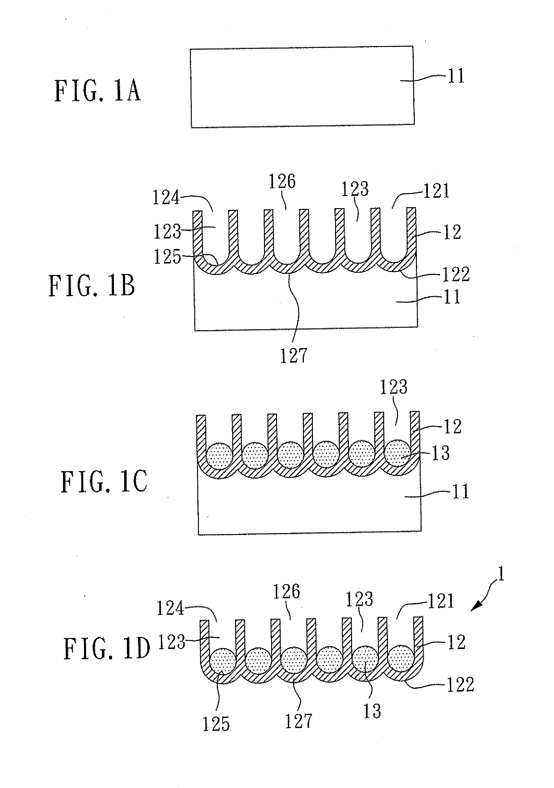
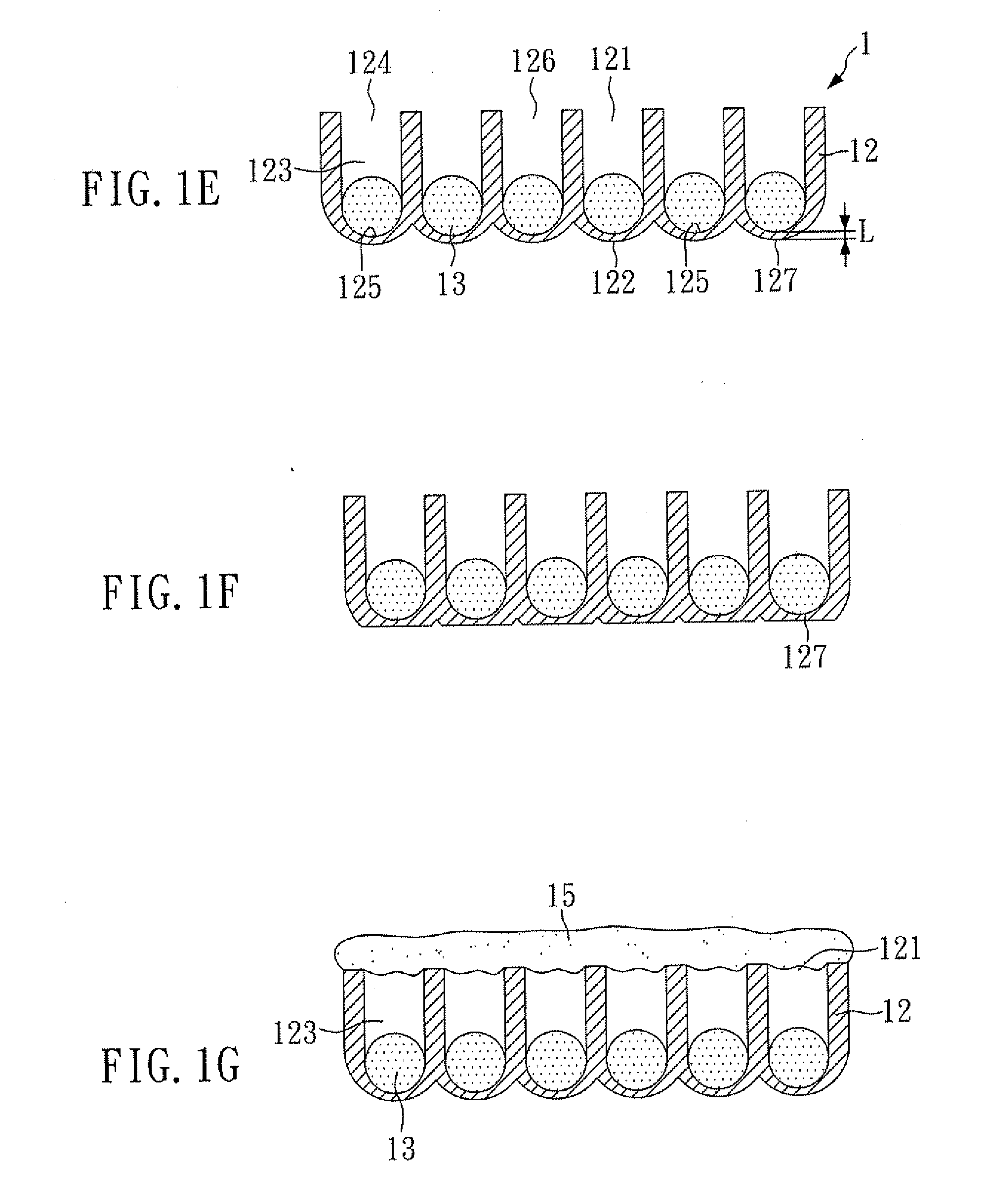
[0058]FIGS. 1A to 1E show a process to manufacture a sensor chip according to the present example. As shown in FIG. 1A, an aluminum plate 11 is first provided in the step (A). Then, as shown in FIG. 1B, the aluminum plate 11 is subjected to an anodizing treatment to form an aluminum oxide film 12 on the surface of the aluminum plate 11 in the step (B). The film 12 is made of a porous material with nano-pores, and has a first surface 121 and a second surface 122 opposite to the first surface 121. In addition, the anodized aluminum oxide film 12 has a plurality of long tube shaped holes 123. Each of the holes 123 has a first end 124 and a second end 125. The first end 124 has an opening 126 at the first surface 121 of the anodized aluminum oxide film 12, while the second end 125 of the hole 123 is closed and located at the second surface 122 of the anodized aluminum oxide film 12. The closed second end 125 is covered by an aluminum oxide layer 127. Subsequently, as shown in FIG. 1C, t...

example 2

[0062]The sensor chip of the present example is manufactured by the same method as illustrated in Example 1, except that the present example uses a physical method (e.g. grinding) to thin the aluminum oxide layer 127 in the step (E), as shown in FIG. 1F.

[0063]In the present example, since no acid reagents are used in the physical method for thinning the aluminum oxide layer 127, the environmental pollution can be reduced. Besides, in the present example, rinsing and drying steps are unnecessary and the method is simpler.

example 3

[0064]After the sensor chip 1 shown in FIG. 1E according to Example 1 is manufactured, a step (F) of forming a passivation layer 15, which may be made of, for example, silicon oxide, on the first surface 121 of the anodized aluminum oxide film 12 is performed, as shown in FIG. 1G. The passivation layer 15 can protect the metal nanoparticles 13 in the holes 123 from being oxidized or prevent the entrance of moisture and impurities.


PUM

PropertyMeasurementUnit
Thicknessaaaaaaaaaa
Thicknessaaaaaaaaaa
Thicknessaaaaaaaaaa

Abstract

The present invention relates to a sensor chip for biomedical and micro-nano structured substances and a method for manufacturing the same. The sensor chip includes plural metal nanoparticles and a porous anodized aluminum oxide film. The plural metal nanoparticles are completely contained in holes of the porous anodized aluminum oxide film and located at the bottom of the holes, and an aluminum oxide layer covering the second end of the holes has a thickness of 1 nm to 300 nm. When analytes such as biomedical molecules are provided in contact with the sensor chip, a Raman signal can be detected based on the Raman spectroscopy. The structure of the sensor chip of the present invention is uncomplicated and the manufacturing steps thereof are simple, and therefore the sensor chip of the present invention is of great commercial value. Also, a method of manufacturing the above sensor chip is disclosed.

Description

CROSS REFERENCE TO RELATED APPLICATION[0001]This application claims the benefits of the Taiwan Patent Application Ser. No. 100103085 filed on Jan. 27, 2011 and the Taiwan Patent Application Ser. No. 100137198 filed on Oct. 13, 2011, and the subject matters of which are incorporated herein by reference.BACKGROUND OF THE INVENTION[0002]1. Field of the Invention[0003]The present invention relates to a sensor chip for biomedical and micro-nano structured substances and a method for manufacturing the same, more particularly, to a sensor chip including a plurality of metal nanoparticles and an anodized aluminum oxide film and a method for manufacturing the same.[0004]2. Description of Related Art[0005]Sensor chips for biomedical and micro-nano structured substances can be applied in drug development, disease and physical assays, DNA sequencing and tissue processing. Sensor chips for biomedical and micro-nano structured substances preferably exhibit high sensitivity, require minimal amount...

Claims


Application Information

Patent Timeline
IPC IPC(8): G01J3/44C25D1/00B82Y40/00
CPCG01N21/658
Inventor TZENG, YON-HUALIU, CHIH-YIHUANG, CHEN-HANLIN, HSING-YINGCHUI, HSIANG-CHENLAU, KYAW-OOCHEN, SHIH-TSEHUANG, CHENG-WEN
Owner NAT CHENG KUNG UNIV
Why Eureka
Try Eureka