Drawing apparatus, drawing method and method of manufacturing article

a technology of drawing apparatus and manufacturing article, applied in the field of drawing apparatus and, can solve the problems of high cost of photolithographic process, insufficient pattern correction, and low reliability of photolithographic process

Inactive Publication Date: 2012-08-30
CANON KK
View PDF2 Cites 36 Cited by
  • Summary
  • Abstract
  • Description
  • Claims
  • Application Information

AI Technical Summary

Benefits of technology

[0013]One disclosed aspect of the embodiments provides, for example, a drawing apparatus advantages in terms of reliability and throughput with which drawing is performed under a design rule. An aspect of the embodiments is a drawing apparatus which performs drawing on a substrate with a plurality of charged particle beams. The apparatus includes: an aperture array which defines a dimension of each of the plurality of charged particle beams on the substrate; a blanker array configured t

Problems solved by technology

As the intended pattern becomes finer and interaction of light becomes more complicated, even the light proximity effect correction is not enough to sufficiently

Method used


Image

  • Drawing apparatus, drawing method and method of manufacturing article
  • Drawing apparatus, drawing method and method of manufacturing article
  • Drawing apparatus, drawing method and method of manufacturing article

Examples


first embodiment

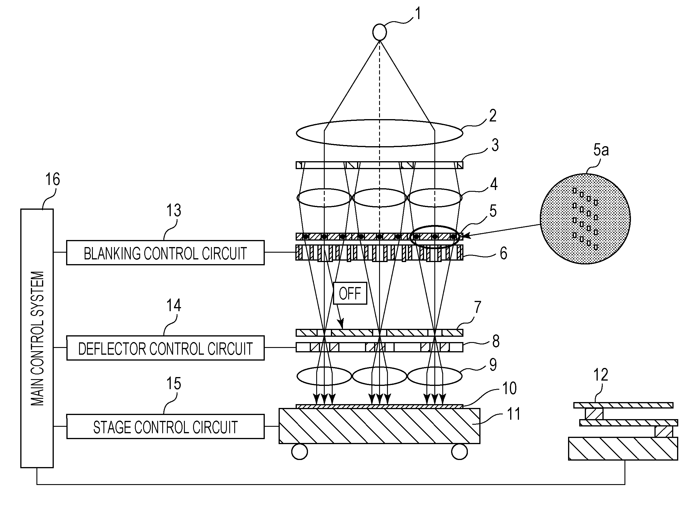
[0027]FIG. 1 illustrates a configuration of a drawing apparatus. In FIG. 1, the reference numeral 1 denotes an electron source, which may be a thermoelectron electron source including LaB6 or BaO / W (i.e., a dispenser cathode) as an electron emission material. The reference numeral 2 denotes a collimating lens which may be an electrostatic lens converging electron beams with the application of an electric field. The electron beams emitted from the electron source 1 become substantially parallel to one another at the collimating lens 2. The drawing apparatuses according to the first and second embodiments draw a pattern on a substrate with a plurality of electron beams. However, charged particle beams, such as ion lines, may be used in place of the electron beams. The drawing apparatuses according to the first and second embodiments may be generalized in drawing apparatuses which draw a pattern on a substrate with a plurality of charged particle beams.

[0028]The reference numeral 3 den...

second embodiment

[0052]The present embodiment relates to a drawing apparatus which draws a 1D-layout intermittent linear pattern. The present embodiment has the same configuration as that of the first embodiment except for the pattern aperture and the scanning grid.

[0053]FIG. 9 illustrates a method of drawing a 1D-layout intermittent linear pattern. As illustrated in “drawing pattern” in FIG. 9, the present embodiment draws intermittent linear patterns CLP arranged in the Y direction at predetermined intervals (e.g., regular intervals) and each extending along a straight line in the X direction. The intermittent linear patterns CLP are arranged at the pitch of 50 nm and the line width of 25 nm in the Y direction. In the intermittent linear pattern CLP, uniformity in the line width in the Y direction is important and the shapes of ends of the linear patterns in the X direction are less important. Therefore, the dimensional accuracy of the intermittent linear pattern CLP needs to be higher in the Y di...

third embodiment

[0059]The method of manufacturing an article according to an embodiment is suitable to manufacture articles, including microdevices, such as semiconductor devices, and devices with fine structures. The manufacturing method may include a process to form a latent image pattern on a photosensitive agent applied to the substrate using the drawing apparatus described above (a process to draw on the substrate), and a process to develop the substrate on which the latent image pattern is formed in the process to draw on the substrate. The manufacturing method may include other known processes (e.g., oxidization, film formation, vapor deposition, doping, smoothing, etching, resist removing, dicing, bonding and packaging). The method of manufacturing an article according to the present embodiment is advantageous in at least one of performance, quality, productivity and production cost of the article as compared with those of the related art method.


PUM


Abstract

A drawing apparatus for drawing on a substrate by a plurality of charged particle beams includes: an aperture array, a blanker array, a scanning mechanism, and a controller. The aperture array specifies the dimension of each of the plurality of charged particle beams on the substrate. The blanker array carries out blanking of the plurality of charged particle beams independently. The scanning mechanism performs a relative scanning between the plurality of charged particle beams and the substrate in each of the first direction and a second direction which cross each other. The controller controls the blanker array at a predetermined pitch on the substrate. The dimension and the pitch are smaller in one of the first direction and the second direction than in the other.

Description

BACKGROUND OF THE INVENTION[0001]1. Field of the Invention[0002]Embodiments of the present invention relate to a drawing apparatus and method that perform drawing on a substrate with a plurality of charged particle beams.[0003]2. Description of the Related Art[0004]In photolithography, as the minimum pattern dimension comes close to the wavelength of a light source, a substrate may be exposed to a pattern which is different from that intended to be due to unintended interaction (i.e., interference) of light. As the intended pattern becomes finer and interaction of light becomes more complicated, even the light proximity effect correction is not enough to sufficiently correct the pattern. In order to solve such a problem, a device design rule in which the width of a pattern is constant and the longitudinal direction of the pattern is limited (hereinafter, “1D-layout”) and a processing method therefor have been proposed (Axelrad, Valery and another, “16 nm with 193 nm Immersion Lithog...

Claims


Application Information

Patent Timeline
IPC IPC(8): G03F7/20H01J3/26
CPCH01J37/3174H01J37/045H01J37/3177B82Y10/00H01J2237/31764H01J2237/31766B82Y40/00H01J2237/0435
Inventor MURAKI, MASATO
Owner CANON KK
Why Eureka
Try Eureka