Nanometric Material Having a Nanopore Enabling High-Sensitivity Molecular Detection and Analysis

a nanopore and nanometric material technology, applied in the field of nanopore configurations, can solve the problems of limiting the sensitivity and resolution with which molecules in the nanopore can be detected and analyzed, and is difficult to achieve in practi

Active Publication Date: 2012-09-20
PRESIDENT & FELLOWS OF HARVARD COLLEGE
View PDF9 Cites 93 Cited by
  • Summary
  • Abstract
  • Description
  • Claims
  • Application Information

AI Technical Summary

Benefits of technology

[0012]These sensor arrangements and sensing methods enable high-resolution, high-sensitivity molecular detection and analysis, thereby achieving sensing of closely-spaced monomers in a polymer and accordingly, sequentially resolving the different ionic blockages caused by each monomer in, for example, a strand of a DNA polymer. Other features and advantages of the invention will be apparent from the following description and accompanying figures, and from the claims.

Problems solved by technology

But this capability has been difficult to achieve in practice, particularly for solid-state nanopore configurations.
It has been found that the length of a solid state nanopore, determined by the thickness of a material layer or layers in which the nanopore is formed, impacts the nature of molecular traversal of the nanopore, and directly limits the sensitivity and the resolution with which molecules in the nanopore can be detected and analyzed.

Method used


Image

  • Nanometric Material Having a Nanopore Enabling High-Sensitivity Molecular Detection and Analysis
  • Nanometric Material Having a Nanopore Enabling High-Sensitivity Molecular Detection and Analysis
  • Nanometric Material Having a Nanopore Enabling High-Sensitivity Molecular Detection and Analysis

Examples


example i

[0053]This example describes an experimental demonstration of a single-layer, bare graphene membrane. A graphene layer was synthesized by CVD on a nickel surface. The nickel was provided as a film by E-beam evaporation on a silicon substrate coated with a layer of SiO2. The nickel layer was thermally annealed to generate a Ni film microstructure with single-crystalline grains of sizes between about a 1 μm and 20 μm. The surfaces of these grains had atomically flat terraces and steps, similar to the surface of single crystal substrates for epitaxial growth. With this topology, the growth of graphene on Ni grains resembles the growth of graphene on the surface of a single crystal substrate.

[0054]In the CVD synthesis, the Ni layer was exposed to H2 and CH4 gases at a temperature of about 1000° C. Raman spectroscopy, transmission electron microscopy and selected area diffraction studies showed the graphene film to be of excellent quality and mostly (87%) a mixture of one and two layer t...

example ii

[0058]This example describes an experimental determination of the conductance of the single-layer, bare graphene membrane of Example I.

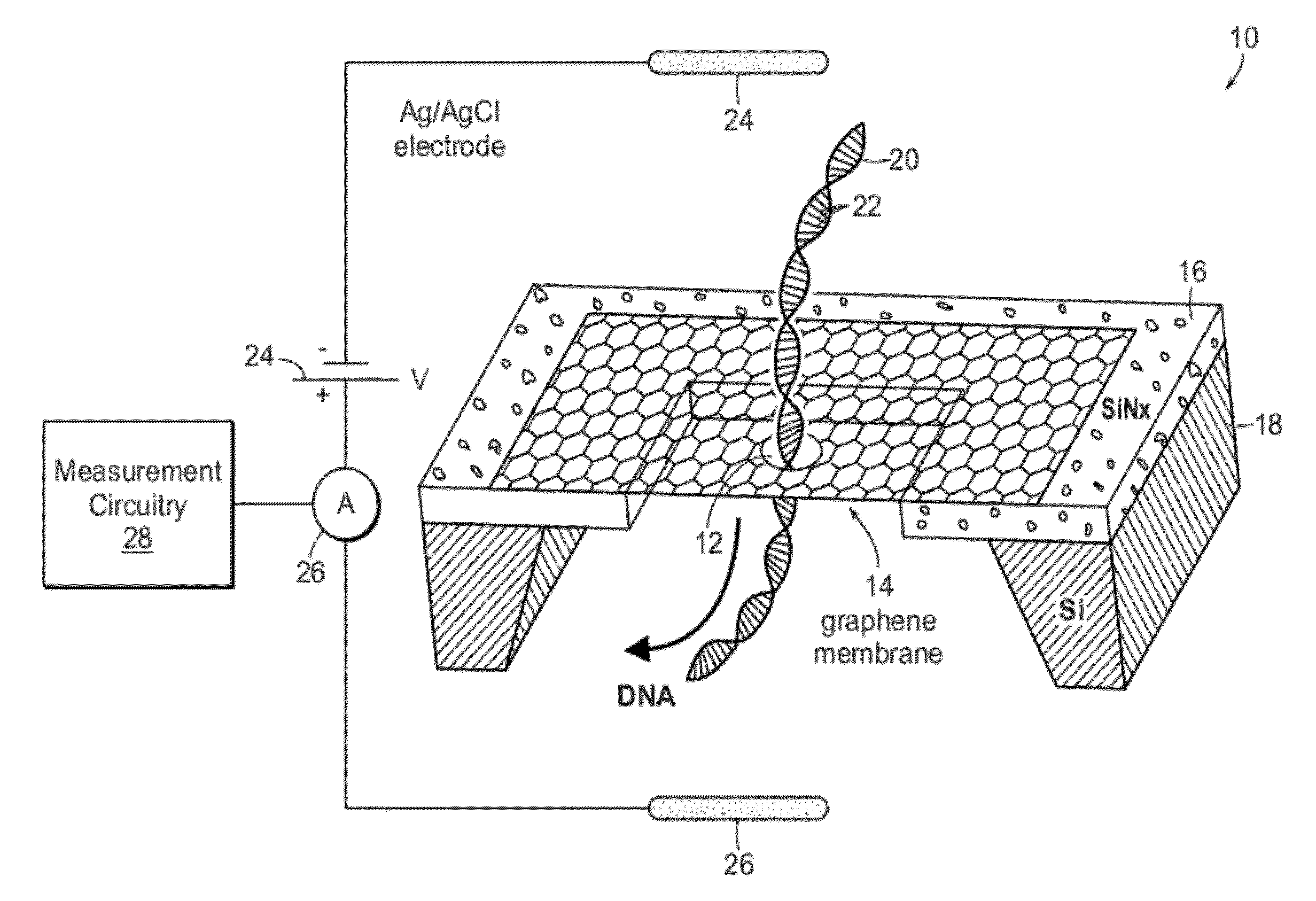
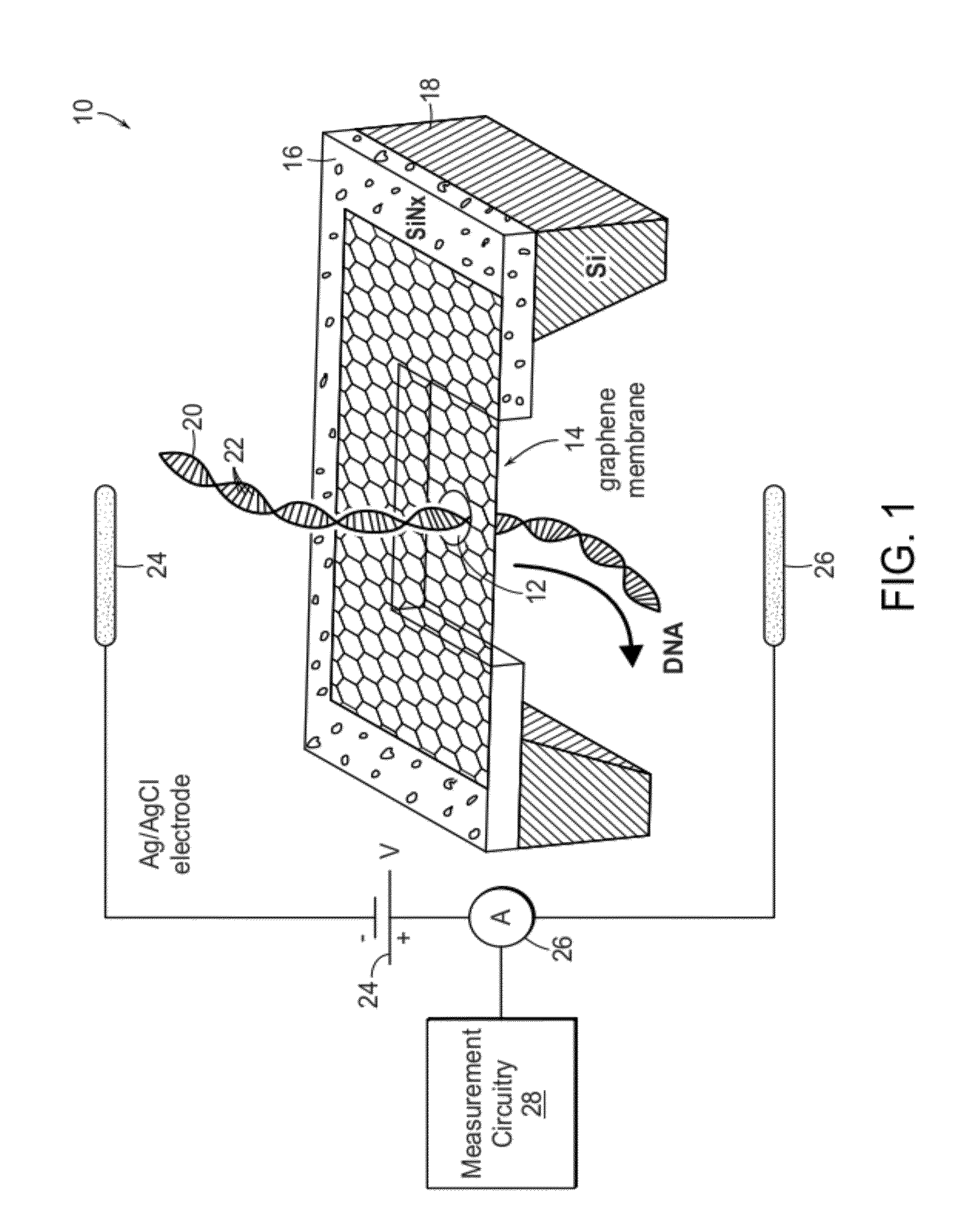
[0059]A chip-mounted single-layer graphene membrane from Example I was inserted between the two half-cells of a custom-built microfluidic cassette made of polyether-etherketone (PEEK). The two sides of the chip were sealed with polydimethylsiloxane (PDMS) gaskets. The opening of the gasket that pressed against the graphene film on the Si / SiNx carrier chip had an inside diameter of ˜100 μm. Consequently, the gasket orifice was smaller than the dimensions of the graphene membrane (0.5×0.5 mm2), and completely sealed off the graphene membrane edge from the electrolyte. On the opposite side of the chip, the electrolyte was in contact with the graphene membrane only through the 200 nm wide square window in SiNx membrane. Note that with this arrangement there was a large area difference between the two graphene membrane faces in contact with the electrolyt...

example iii

[0065]This example describes an experimental determination of the conductance of the single-layer, bare graphene membrane of Example I including a nanopore.

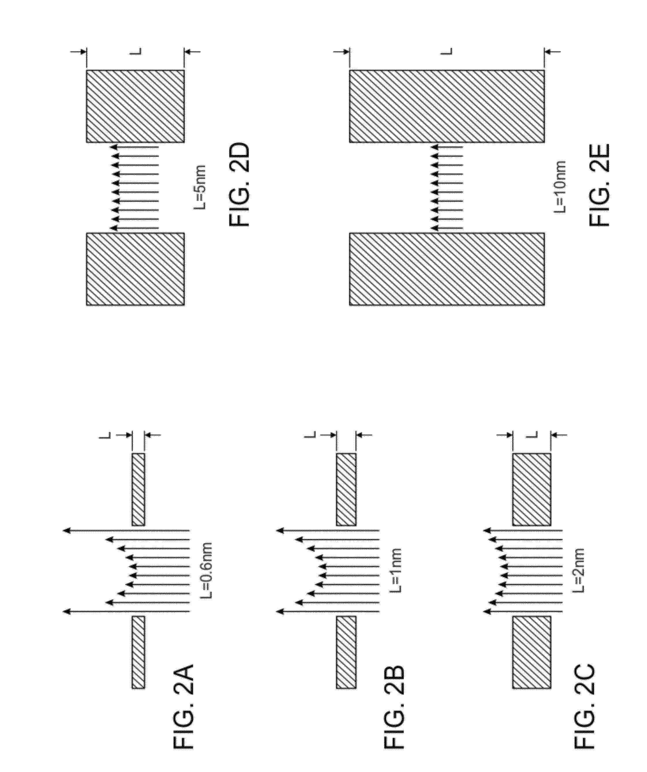
[0066]A single nanometer-sized nanopore was drilled through several of the graphene membranes of Example I using a focused electron beam in a JEOL 2010 FEG transmission electron microscope operated at 200 kV acceleration voltage. The nanopore diameter was determined by EM visualization in a well-spread electron beam so as to keep the total electron exposure of the graphene membrane to a minimum. A nanopore diameter of 8 nm was determined as the average of 4 measurements along different nanopore axes, as determined from calibrated TE micrographs using DigitalMicrograph software (Gatan, Inc.). If the chip or TEM holder had any contaminating organic residue, amorphous carbon was seen to visibly deposit under the electron beam. Such devices were discarded. After drilling the nanopore, the graphene nanopore chips that were not immedia...


PUM

PropertyMeasurementUnit
diameteraaaaaaaaaa
diameteraaaaaaaaaa
diameteraaaaaaaaaa

Abstract

There is provided a substantially bare, self-supported single-layer graphene membrane including a nanopore extending through a thickness of the graphene membrane from a first to a second membrane surface opposite the first graphene membrane surface. A connection from the first graphene membrane surface to a first reservoir provides, at the first graphene membrane surface, a species in an ionic solution to the nanopore, and a connection from the second graphene membrane surface to a second reservoir is provided to collect the species and ionic solution after translocation of the species and ionic solution through the nanopore from the first graphene membrane surface to the second graphene membrane surface. An electrical circuit is connected on opposite sides of the nanopore to measure flow of ionic current through the nanopore in the graphene membrane.

Description

CROSS-REFERENCE TO RELATED APPLICATIONS[0001]This is a continuation-in-part of co-pending International Application PCT / US / 2010 / 049238, with an international filing date of Sep. 17, 2010. This application claims the benefit of U.S. Provisional Application No. 61 / 243,607, filed Sep. 18, 2009, the entirety of which is hereby incorporated by reference. This application also claims the benefit of U.S. Provisional Application No. 61 / 355,528, filed Jun. 16, 2010, the entirety of which is hereby incorporated by reference.STATEMENT REGARDING FEDERALLY SPONSORED RESEARCH[0002]This invention was made with Government support under Contract No. 2R01HG003703-04 awarded by the NIH. The Government has certain rights in the invention.BACKGROUND[0003]This invention relates generally to molecular detection and analysis, and more particularly relates to configurations for a nanopore arranged to detect molecules translocating through the nanopore.[0004]The detection, characterization, identification, a...

Claims


Application Information

Patent Timeline
Patent Type & Authority Applications(United States)
IPC IPC(8): G01N27/447G01N27/453B82Y5/00B82Y30/00B82Y99/00
CPCB82Y30/00G01N15/1056C12Q2565/631G01N33/48721G01N2015/0038G01N15/12G01N27/44704G01N33/48C12Q1/6869
Inventor GARAJ, SLAVENGOLOVCHENKO, JENE A.BRANTON, DANIEL
Owner PRESIDENT & FELLOWS OF HARVARD COLLEGE
Why Eureka
Try Eureka