Organic photovoltaic cell incorporating electron conducting exciton blocking layers

Active Publication Date: 2012-09-20
RGT UNIV OF MICHIGAN
View PDF33 Cites 52 Cited by
  • Summary
  • Abstract
  • Description
  • Claims
  • Application Information

AI Technical Summary

Benefits of technology

[0057]The present disclosure is further directed to a method of increasing the power conversion efficiency of

Problems solved by technology

As a general rule, a photovoltaic cell provides power to a circuit, device or equipment, but does not provide a signal or current to control detection circuitry, or the output of information from the detection circuitry.
In contrast, a photodetector or photoconductor provides a signal or current to control detection circuitry, or the output of information from the detection circuitry but does not provide power to the circuitry, device or equipment.
However, efficient crystalline-based devices, especially of large surface area, are difficult and expensive to produce due to the problems inherent in producing large crystals without significant efficienc

Method used


Image

  • Organic photovoltaic cell incorporating electron conducting exciton blocking layers
  • Organic photovoltaic cell incorporating electron conducting exciton blocking layers
  • Organic photovoltaic cell incorporating electron conducting exciton blocking layers

Examples


example 1

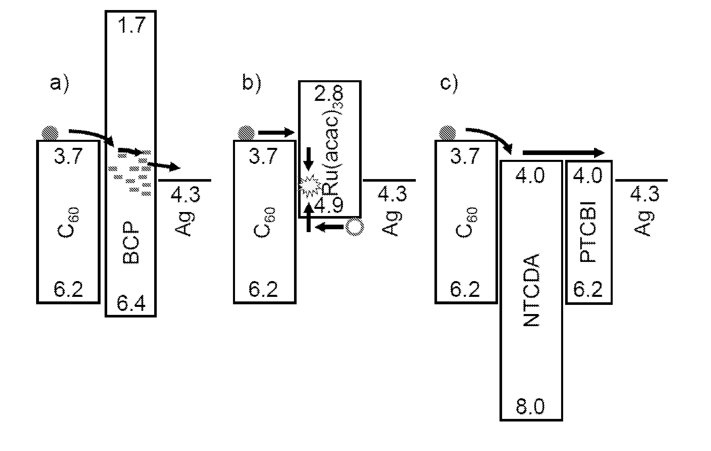
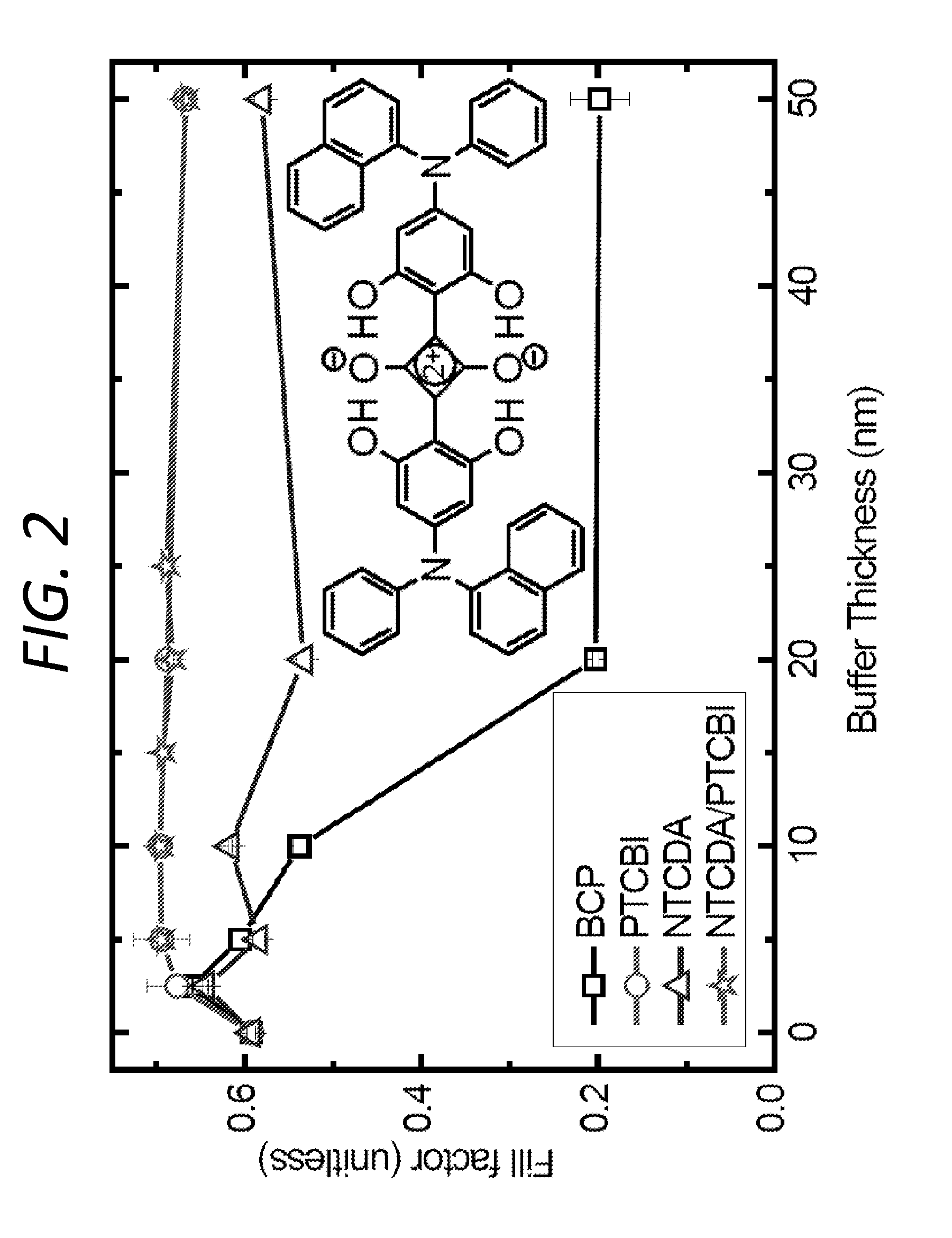
[0085]Devices were grown on 150 nm thick layers of indium tin oxide (ITO) pre-coated onto glass substrates. Prior to deposition, the ITO surface was cleaned in a surfactant and a series of solvents and then exposed to ultraviolet-ozone for 10 min before loading into a high vacuum chamber (base pressure −7 Torr) where MoO3 was thermally evaporated at ˜0.1 nm / s. Substrates were then transferred to a N2 glovebox where 2,4-bis[4-(N-Phenyl-1-naphthylamino)-2,6-dihydroxyphenyl]squaraine (1-NPSQ, see molecular structural formula in FIG. 2, inset) films were spin-coated from heated 6.5 mg / ml solutions in 1,2-dichlorobenzene, and thermally annealed on a hot plate at 110° C. for 5 min to promote the growth of a nanocrystalline morphology.

[0086]Substrates were once again transferred into the high vacuum chamber for deposition of purified organics at 0.1 nm / s, followed by a 100 nm thick Ag cathode deposited at 0.1 nm / s through a shadow mask with an array of 1 mm diameter openings. Current densi...


PUM


Abstract

The present disclosure relates to photosensitive optoelectronic devices comprising a compound blocking layer located between an acceptor material and a cathode, the compound blocking layer comprising: at least one electron conducting material, and at least one wide-gap electron conducting exciton blocking layer. For example, 3,4,9,10 perylenetetracarboxylic bisbenzimidazole (PTCBI) and 1,4,5,8-napthalene-tetracarboxylic-dianhydride (NTCDA) function as electron conducting and exciton blocking layers when interposed between the acceptor layer and cathode. Both materials serve as efficient electron conductors, leading to a fill factor as high as 0.70. By using an NTCDA/PTCBI compound blocking layer structure increased power conversion efficiency is achieved, compared to an analogous device using a conventional blocking layers shown to conduct electrons via damage-induced midgap states.

Description

CROSS-REFERENCE TO RELATED APPLICATION[0001]This application claims the benefit of priority to U.S. Provisional Application No. 61 / 444,899, filed on Feb. 21, 2011, and U.S. Provisional Application No. 61 / 479,237, filed on Apr. 26, 2011, both of which are incorporated herein by reference in their entireties.STATEMENT REGARDING FEDERALLY SPONSORED RESEARCH[0002]This invention was made with U.S. Government support under DE-SC00000957 and DE-SC0001013, both awarded by the U.S. Department of Energy. The government has certain rights in the invention.JOINT RESEARCH AGREEMENT[0003]The claimed invention was made by, on behalf of, and / or in connection with one or more of the following parties to a joint university-corporation research agreement: University of Michigan, and Global Photonic Energy Corporation. The agreement was in effect on and before the date the invention was made, and the claimed invention was made as a result of activities undertaken within the scope of the agreement.FIELD...

Claims


Application Information

Patent Timeline
IPC IPC(8): H01L51/54H01L51/56
CPCB82Y10/00H01L51/0046H01L51/0047H01L51/0053Y02E10/549H01L51/0078H01L51/4246H01L2251/308H01L51/006H10K85/211H10K85/215H10K85/621H10K85/633H10K85/311H10K30/211H10K2102/103H10K30/50Y02P70/50H10K30/81H10K2102/00H10K2102/351
Inventor FORREST, STEPHEN R.LASSITER, BRIAN E.
Owner RGT UNIV OF MICHIGAN
Why Eureka
Try Eureka