Sic semiconductor element and manufacturing method for same

a semiconductor element and manufacturing method technology, applied in the field of semiconductor element and manufacturing method for same, can solve the problems of increased power consumption, low channel mobility of mis(mos)fet of sic, etc., to improve channel mobility, reduce interface defects (interface state density), and improve channel mobility.

Active Publication Date: 2012-09-27
NARA INSTITUTE OF SCIENCE AND TECHNOLOGY
View PDF1 Cites 26 Cited by
  • Summary
  • Abstract
  • Description
  • Claims
  • Application Information

AI Technical Summary

Benefits of technology

[0052]According to the present invention, by performing the heat treatment on the insulating film using the phosphorus-containing gas, there is an effect of being able to drastically reduce interface defects (interface state density) of the insulating film and SiC and make the channel mobility dramatically better than before. By improving the channel mobility, there is an effect of reducing power consumption of a power device using the present invention. Further, a surface passivation film using the present invention has an effect of achieving a reduction in leakage current and an improvement in amplification factor.

Problems solved by technology

However, it has been conventionally problematic that there are many defects in an interface between a gate insulating film (gate oxide film) and SiC and channel mobility is low in MIS (MOS) FETs of SiC.
The channel mobility of the MIS(MOS)FET of SiC is low because there are many defects in the interface of SiC produced by conventional technologies, i.e. interface state density is high.
If the on-resistance value of the transistor increases, power consumption increases.
That is, by device integration, the potential of SiC originally having a high electron mobility cannot be utilized at all.
However, the above patent literature 1 has a problem that reliability of the insulating film provided on an SiC substrate is poor since nitrogen or phosphorus is ion-implanted into SiC immediately below the gate insulating film or the epitaxial growth is allowed.
There is also a problem in controllability of impurity concentration and film thickness of epi-layer.
Resulting from that, there is also a problem that the channel mobility and a threshold voltage vary.
There is also a problem that an effective range of a process condition is narrow.

Method used


Image

  • Sic semiconductor element and manufacturing method for same
  • Sic semiconductor element and manufacturing method for same
  • Sic semiconductor element and manufacturing method for same

Examples


embodiment 1

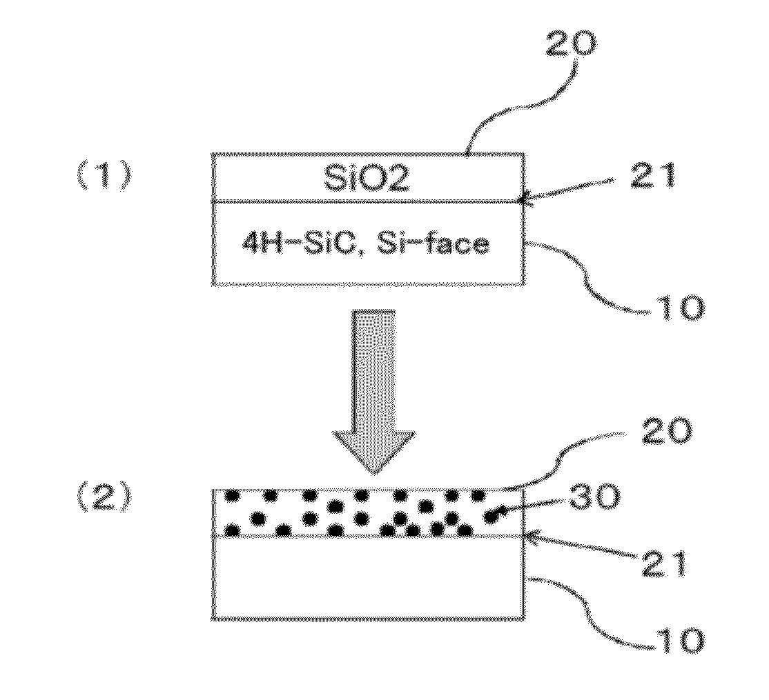
[0076]The manufacturing method of a first example is described using FIGS. 4 and 5. FIGS. 4 show a state where a gate insulating film 20 is formed on an SiC semiconductor 10 and phosphorus is added to that gate insulating film 20. Here is illustrated an example using an oxide film (SiO2) as an insulating film. In FIG. 4 (2), phosphorus 30 has reached up to an interface 21 between the insulating film and SiC. By the phosphorus 30 having reached up to the interface 21 between the insulating film and SiC, interface defects can be reduced and the channel mobility can be improved.

[0077]Phosphorus is added to the insulating film on the SiC substrate in a procedure shown in FIG. 5. First, the insulating film is formed on the SiC substrate (S10) and then phosphorus is added to the insulating film (S20). Subsequently, a diffusing step is performed (S25) to cause phosphorus to reliably reach the interface 21 between the insulating film and the SiC.

[0078]The procedure of adding phosphorus to t...


PUM


Abstract

Disclosed are an SiC semiconductor element and manufacturing method for an SiC semiconductor element in which the interface state density of the interface of the insulating film and the SiC is reduced, and channel mobility is improved. Phosphorus (30) is added to an insulating film (20) formed on an SiC semiconductor (10) substrate in a semiconductor element. The addition of phosphorous to the insulating film makes it possible to significantly reduce the defects (interface state density) in the interface (21) of the insulating film and the SiC, and to dramatically improve the channel mobility when compared with conventional SiC semiconductor elements. The addition of phosphorus to the insulating film is carried out by heat treatment. The use of heat treatment to add phosphorous to the insulating film makes it possible to maintain the reliability of the insulating film, and to avoid variation in channel mobility and threshold voltage.

Description

TECHNICAL FIELD [0001]The present invention relates to a technology for reducing interface defects on an insulating film (oxide film) and an SiC semiconductor of an SiC semiconductor element and improving channel mobility of a MISFET (MIS field-effect transistor), a MOSFET (MOS field-effect transistor) or the like.BACKGROUND ART [0002]An SiC semiconductor is a semiconductor made of SiC (silicon carbide) which is a compound of carbon (C) and silicon (Si). A most distinctive feature of the SiC semiconductor is to have a physical value suitable as a material of semiconductor devices (power devices) used in power electronics. For example, in the case of commercially available single-crystal 4H-SiC, a band gap is 3.3 eV which is three times as wide as conventional Si-semiconductors, dielectric breakdown field strength is 3 MV / cm which is about ten times as high as conventional Si-semiconductors and saturation electron velocity is three times as fast as conventional Si-semiconductors. Fur...

Claims


Application Information

Patent Timeline
Patent Type & Authority Applications(United States)
IPC IPC(8): H01L29/38H01L21/265
CPCH01L21/049H01L29/1608H01L29/51H01L29/518H01L29/94H01L29/66068H01L29/78H01L29/7802H01L29/6606
Inventor YANO, HIROSHIOKAMOTO, DAI
Owner NARA INSTITUTE OF SCIENCE AND TECHNOLOGY
Why Eureka
Try Eureka