

Nitride semiconductor light-emitting device and production method thereof
- Summary
- Abstract
- Description
- Claims
- Application Information
AI Technical Summary
Benefits of technology
Problems solved by technology
Method used
Image

Examples
embodiment 1
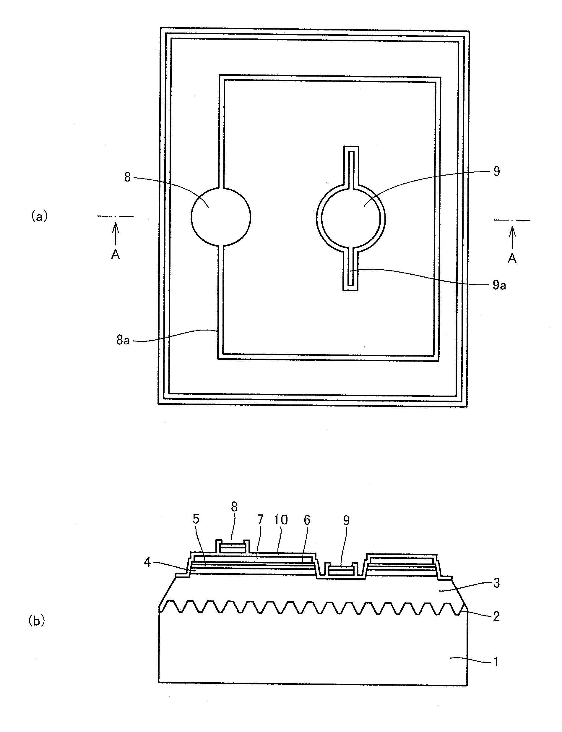
[0081]In a method of producing a nitride semiconductor light-emitting device according to Embodiment 1, an n-type nitride semiconductor layer 3 is deposited on a substrate 1 of sapphire having a main surface of a (0001) plane orientation for example with a buffer layer 2 of AlN intervening therebetween, as shown in FIG. 1(b). This n-type nitride semiconductor layer 3 includes a GaN underlayer of 9 μm thickness and an Si-doped n-type GaN contact layer (carrier concentration: about 6×1018 cm−3) deposited at a substrate temperature of about 1000° C. and has sheet resistance Rs1 of about 6-8 Ω / □.
[0082]An active layer 4 is deposited on n-type nitride semiconductor layer 3. This active layer 4 has a multiple-quantum-well structure in which n-type In0.15Ga0.85N quantum well layers each having a thickness of 3.5 nm and Si-doped GaN barrier layers each having a thickness of 6 nm are deposited six times repeatedly at a substrate temperature of about 890° C., for example.
[0083]On active layer ...
embodiment 2
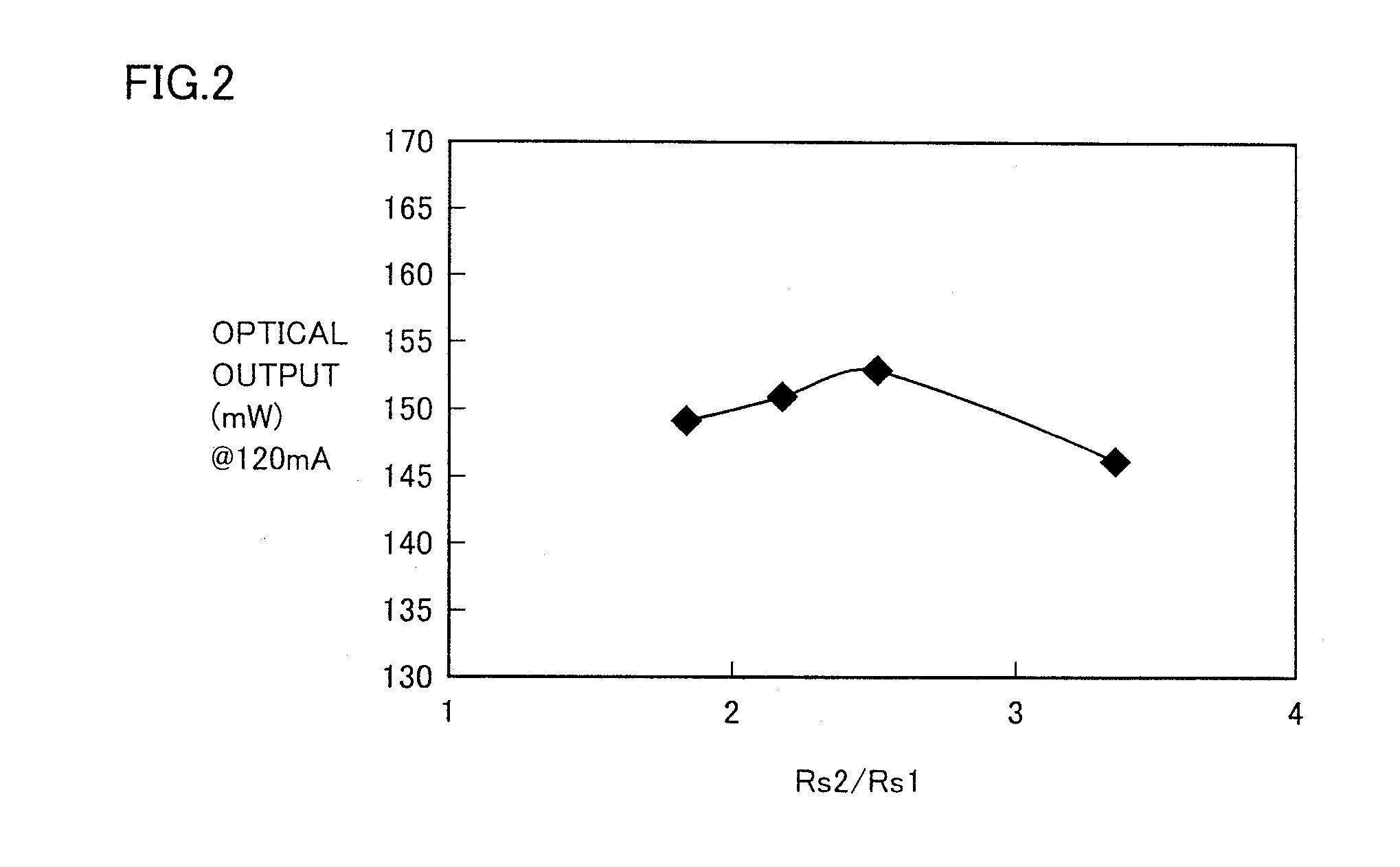
[0090]In a method of producing a nitride semiconductor light-emitting device according to Embodiment 2 of the present invention, the second annealing after deposition of the ITO current diffusion layer is conducted in the vacuum atmosphere for 5 minutes at a temperature of 430° C. decreased as compared with Embodiment 1. As a result, sheet resistance Rs2 is increased to 13Ω / □, while contact resistance Rc between the ITO current diffusion layer and the p-type contact layer of p-type GaN is decreased to 0.04 Ω·cm2. It is considered that sheet resistance Rs2 is increased as compared with Embodiment 1 because the crystallinity of the current diffusion layer is lowered. In the meantime, it is considered that contact resistance Rc between the current diffusion layer and the p-type contact layer of p-type GaN is decreased as compared with Embodiment 1 because the height of the Schottky barrier is lowered.
[0091]Further, the optical output at 120 mA in Embodiment 2 is increased as compared w...
embodiment 3
[0093]In a method of producing a nitride semiconductor light-emitting device according to Embodiment 3 of the present invention, the second annealing after deposition of the ITO current diffusion layer is conducted in the vacuum atmosphere for minutes at an annealing temperature of 410° C. further decreased as compared with Embodiments 1 and 2. As a result, sheet resistance Rs2 is increased to 15Ω / □, while contact resistance Rc between the ITO current diffusion layer and the p-type contact layer of p-type GaN is decreased to 0.03 Ω·cm2. Further, the optical output at 120 mA in this Embodiment 3 is increased to the highest and therefore it is understood that the second annealing temperature is most optimized.
PUM
 Abstract
Description
Claims
Application Information