Method of manufacturing a transfer mask and method of manufacturing a semiconductor device

a manufacturing method and semiconductor technology, applied in the field of manufacturing a transfer mask and manufacturing a semiconductor device, can solve the problems of difficult to identify the internal defect, difficult to detect the internal defect in the subsequent transfer mask manufacturing process, and new generation of processes, so as to achieve the effect of not reducing the yield

Active Publication Date: 2012-10-04
HOYA CORP
View PDF0 Cites 0 Cited by
  • Summary
  • Abstract
  • Description
  • Claims
  • Application Information

AI Technical Summary

Benefits of technology

[0057]According to this aspect, since the transfer mask manufactured by the method according to any one of the above-mentioned aspects (1) to (11) is used, the yield is not reduced even when forming a circuit pattern on a semiconductor wafer by photolithography. This is particularly effective when forming a circuit pattern on a semiconductor wafer by photolithography using laser exposure light having a wavelength of 200 nm or less.
[0058]According to this invention, it is possible to provide a method of manufacturing a transfer mask with no defect by detecting, in addit

Problems solved by technology

Accordingly, there may be a possibility that after the transparent substrate before the formation of the thin film is inspected for the presence or absence of an internal defect, an internal defect is newly generated in those processes described above.
On the other hand, if the transparent substrate having an internal defect is erroneously judged to be satisfactory in an internal defect inspection and is then thrown into the mask blank manufacturing processes, it is difficult to detect the internal defect in the mask blank manufacturing processes or the subsequent transfer mask manufacturing processes.
Thus, it is difficult to identify the internal defect only based on the transmittance distribution, i.e. the transmitted light quantit

Method used


Image

  • Method of manufacturing a transfer mask and method of manufacturing a semiconductor device
  • Method of manufacturing a transfer mask and method of manufacturing a semiconductor device
  • Method of manufacturing a transfer mask and method of manufacturing a semiconductor device

Examples


Embodiment Construction

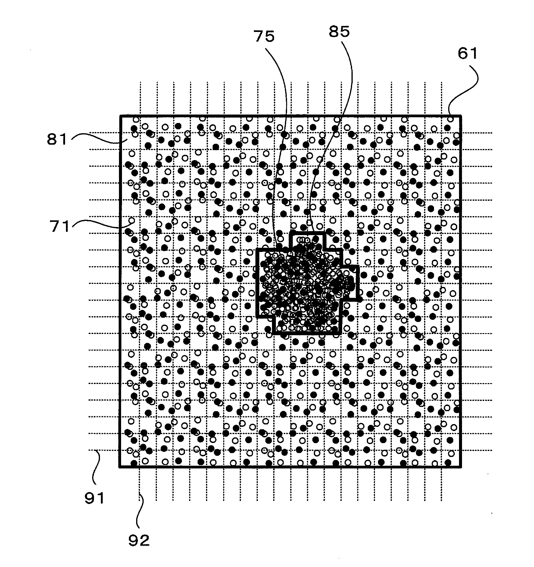
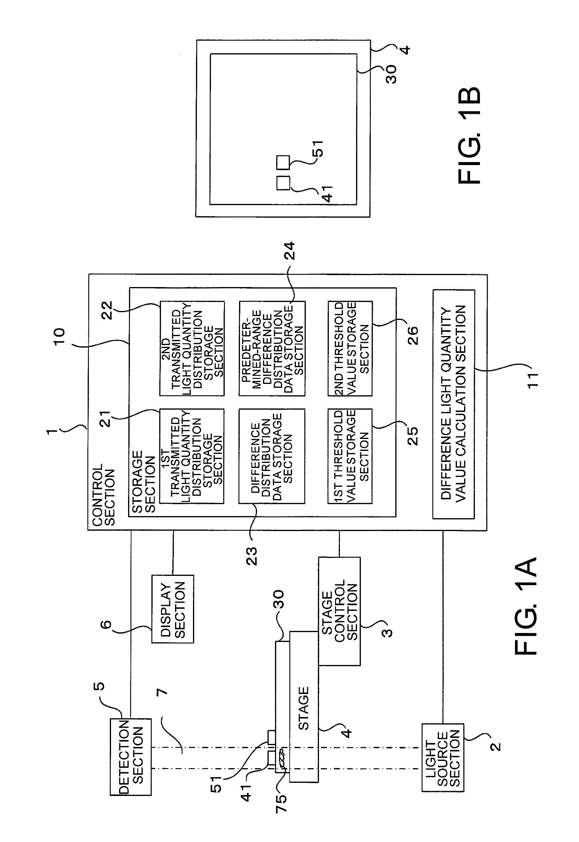
[0064]Referring to FIGS. 1A and 1B, according to an embodiment of this invention, an inspection apparatus for a transfer mask 30 comprises a light source section 2 for emitting laser light, a stage 4, a detection section 5, and a control section 1 and senses or detects an internal defect 75 (optically nonuniform region that causes a local change in optical properties in pattern transfer). Although a method of detecting the presence or absence of an internal defect of a transparent substrate will be described hereinbelow, detection of the presence or absence of a foreign matter defect adhering to a main surface, on the side opposite to a main surface where a thin film is formed, of the transparent substrate and detection of the presence or absence of a foreign matter defect adhering to a surface of a pellicle attached to the thin film can also be carried out by the same method.

[0065]The control section 1 controls the entire inspection apparatus and is also a detection means which is ...


PUM


Abstract

An internal defect or the like of a transfer mask is detected using transmitted light quantity distribution data of an inspection apparatus. Using a die-to-die comparison inspection method, inspection light is irradiated to a first region of a thin film to obtain a first transmitted light quantity distribution, the inspection light is also irradiated to a second region of the thin film to obtain a second transmitted light quantity distribution, a predetermined-range difference distribution is produced by plotting coordinates at which difference light quantity values calculated from a comparison between the first transmitted light quantity distribution and the second transmitted light quantity distribution are each not less than a first threshold value and less than a second threshold value, and a selection is made of a transfer mask in which a region with high density of plotting is not detected in the predetermined-range difference distribution.

Description

[0001]This application is based upon and claims the benefit of priority from Japanese Patent Application No. 2011-080203, filed Mar. 31, 2011, the disclosure of which is incorporated herein in its entirety by reference.BACKGROUND OF THE INVENTION[0002]This invention relates to a method of manufacturing a transfer mask having, on a transparent substrate, a thin film formed with a transfer pattern and further relates to a method of manufacturing a semiconductor device using this transfer mask.[0003]A transfer mask (photomask) is used for forming a substrate pattern on a semiconductor substrate (wafer) or the like in the manufacture of a semiconductor element or a liquid crystal display. The substrate pattern is formed by photolithography, i.e. by transmitting exposure light from a light source through the transfer mask to transfer a mask pattern of the transfer mask to an object (e.g. a resist film on the semiconductor wafer), then developing the object, and then carrying out etching ...

Claims


Application Information

Patent Timeline
IPC IPC(8): G03F1/84G03F7/20
CPCG03F1/84G03F1/72G03F1/70G03F1/76H01L21/0273
Inventor TANABE, MASARUMITSUI, HIDEAKINISHIDA, NAOKIIWASHITA, SATOSHI
Owner HOYA CORP
Why Eureka
Try Eureka