Photo detector array of geiger mode avalanche photodiodes for computed tomography systems

a computed tomography and photodiode technology, applied in the field of semiconductor photodetectors, can solve the problems of inability to provide data or feedback as to the number and/or energy of photons detected, inability to provide energy discriminatory data or otherwise count the number and/or energy of photons actually received by a given detector element or pixel, and achieve accurate counting of received photons. high gain, low noise

Active Publication Date: 2012-10-25
STMICROELECTRONICS SRL
View PDF8 Cites 23 Cited by
  • Summary
  • Abstract
  • Description
  • Claims
  • Application Information

AI Technical Summary

Benefits of technology

[0015]A photon counting energy discriminating CT detector, to be capable of preventing saturation at the x-ray photon flux rates typically found in conventional CT systems, should generate very short pulses with high gain and low noise. This would prevent superposition of pulse waveforms, thus an accurate counting of received photons and a reliable estimation of their energy. This is accomplished in an effective and efficient manner in a photo detector array of Geiger mode avalanche photodiodes disclosed herein.

Problems solved by technology

However, CT involves a considerably greater amount of radiation than conventional radiography.
A drawback of such detectors however is their inability to provide data or feedback as to the number and / or energy of photons detected.
A drawback of these detectors is their inability to provide energy discriminatory data or otherwise count the number and / or measure the energy of photons actually received by a given detector element or pixel.
Under the charge integration operation mode, the photodiode is not capable of discriminating between the energy level or the photon count from the scintillation.
However, there are varying problems that limit the use of these detectors.
In the case of APDs, there is additional gain need to enable photon counting, but with associated gain-instability noise, temperature sensitivity, and other reliability issues.
In the case of photomultiplier tubes, these devices are too large, mechanically fragile, and costly for high resolution detectors covering large areas as used in CT.
As such, these photomultiplier tubes have been limited to use in PET or SPECT systems.
A drawback of direct conversion semiconductor detectors, however, is that these types of detectors cannot count at the x-ray photon flux rates typically encountered with conventional CT systems.
The very high x-ray photon flux rate causes pile-up and polarization.
This type of pile-up results in a degradation of the energy resolution of the system.
In the second type of pile-up, the two or more events arrive close enough in time so that the system is not able to resolve them as distinct events.
In addition, pile-up leads to a more or less pronounced depression of counts in high x-ray flux, resulting in detector quantum efficiency (DQE) loss.
Direct conversion detectors are also susceptible to a phenomenon called “polarization” where charge trapping inside the material changes the internal electric field, alters the detector count and energy response in an unpredictable way, and results in hysteresis where response is altered by previous exposure history.
Above these thresholds, the detector response is not predictable and has degraded dose utilization that leads to loss of imaging information and results in noise and artifacts in x-ray projection and CT images.
What can be problematic, however, is that the bowtie filter may not be optimal given that a subject population is significantly less than uniform and can vary in shape.
Low x-ray flux in the projection will ultimately contribute to noise in the reconstructed image of the subject.
However, the signal-to-noise ratio of the resulting signal may be reduced, and the level of cross-talk will be disadvantageously significant due to the increased perimeter between sub-pixels.
Charge sharing may cause the photon to be missed entirely or mislabeled in energy.

Method used


Image

  • Photo detector array of geiger mode avalanche photodiodes for computed tomography systems
  • Photo detector array of geiger mode avalanche photodiodes for computed tomography systems
  • Photo detector array of geiger mode avalanche photodiodes for computed tomography systems

Examples


Embodiment Construction

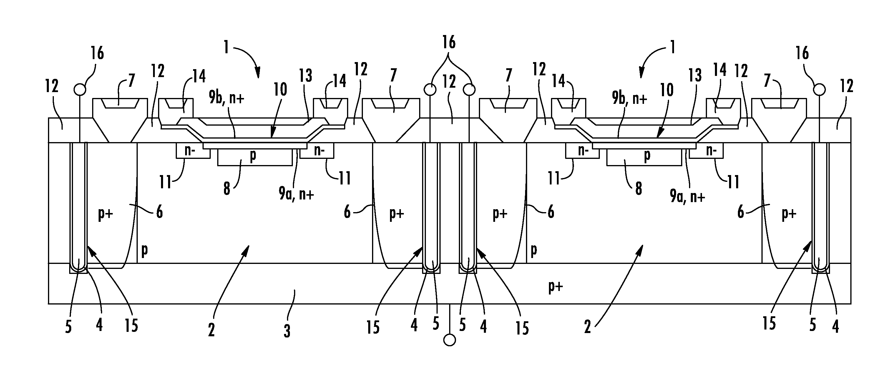
[0026]An exemplary structure of an array of Geiger-mode avalanche photodiodes (GMAP) is schematically illustrated in FIG. 1. In the depicted example, only two photodiodes are shown, though the array may comprise any number of photodiodes organized in rows and columns. The avalanche photodiode has three terminals instead of two: a cathode contact 14, an anode contact 7, a metal structure 5 having an output terminal 16 on which spikes correlated to avalanche events of the photodiode may be sensed. The metal structure 5 is defined in a trench coated with a dielectric 4, preferably silicon oxide, and is thus capacitively coupled with a region of the photodiode, that in the shown example is the anode diffusion 6.

[0027]The GMAP active area is defined by the p enrichment diffusion 8 (anode); this enrichment diffusion 8 identifies also the high electric field active region. The anode is contacted by a metal bus connected to p+ anode contact layer 6 or by a back-side metallization of the p+ ...


PUM


Abstract

The photo detector array is configured to generate pulses with short rise and fall times because each Geiger mode avalanche photodiode includes an anode contact, a cathode contact, an output contact electrically insulated from the anode and cathode contacts, a semiconductor layer, and at least one shield or metal structure in the semiconductor layer capacitively coupled to the semiconductor layer and coupled to the output contact. The output contacts of all Geiger mode avalanche photodiodes are connected in common and are configured to provide for detection of spikes correlated to avalanche events on any avalanche photodiode of the array.

Description

RELATED APPLICATIONS[0001]This application is a Continuation-in-Part (CIP) application of copending U.S. patent application Ser. No. 13 / 053,595 filed Mar. 22, 2011, the entire disclosure of which is incorporated herein by reference.FIELD OF THE INVENTION[0002]The present application relates to semiconductor photodetectors and, more precisely, to an array of Geiger-mode avalanche photodiodes for a computed tomography system configured to count received photons and determine the energy of radiation impinging on the array.BACKGROUND OF THE INVENTION[0003]Computed Tomography (CT) is a known approach for obtaining images of the internal structure of a subject from its projections. CT has been shown to be an advancement compared to conventional radiography in the detection of a wide variety of diseases because of the greater contrast it achieves. However, CT involves a considerably greater amount of radiation than conventional radiography. See R. Lecomte, P. Berard, Cadorette, D. Lapointe...

Claims


Application Information

Patent Timeline
Patent Type & Authority Applications(United States)
IPC IPC(8): H01L27/146H01L31/107
CPCH01L27/1446H01L31/107H01L27/14689
Inventor SANFILIPPO, DELFO NUNZIATOCONDORELLI, GIOVANNI
Owner STMICROELECTRONICS SRL
Why Eureka
Try Eureka