Device for storing and processing information (spi device)

a technology for storing and processing information, applied in the field of radio electronics, computation, informatics, and telecommunications, can solve the problems of reducing the protection of radio components and switchability, not having protection against adverse environmental impacts, and known devices having certain limitations, so as to achieve reliable conductive mechanical junction

Active Publication Date: 2012-10-25
LEONTIEV VLADIMIR VASILIEVICH +1
View PDF7 Cites 38 Cited by
  • Summary
  • Abstract
  • Description
  • Claims
  • Application Information

AI Technical Summary

Benefits of technology

[0024]The communication board coils can be in the form of inductance coils. The logic board and microelectronic units (MEU) can comprise semiconductor devices (SCD), passive radio components (REC), and heat sinks. MEU, SCD, and other REC can be provided on one side or both sides of the switching board of the logic board. In this case, microelectronic units and SCD can be selectively provided with heat sinks. Said heat sinks can be electrically isolated from the base, switching layers of the logic board, microelectronic units, SCD and radio components, and can have a heat link with a base through heat-conductive dielectric material filling in the space between the base and the heat sink. The logic board is provided on the base so that the microelectronic units and the radio components are faced towards the space between stiffener ribs of the base. The space between the logic board components and a base is filled with a heat conductive damping dielectric material. The heat sinks can be implemented with a heat link. Moreover, the magnetic core is installed adjacent to the logic board and / or base and divided into at least two magnetic cores, the at least two magnetic cores being installed adjacent and parallel to switching layers of the communication boards and corresponding communication coils. The magnetic core can comprise at least one layer of conductive magnetic material. The magnetic core corresponding to power supply channel communication coils is electrically isolated from the magnetic core corresponding to information channel communication coils. Additionally, the SPI unit can be provided with a common bus electrically connecting with the magnetic core, and also comprises at least one logic board each comprising a switching board with the microelectronic units of the switching board, SCD, other radio components and heat sinks, if required. The base is provided with stiffener ribs from one or both sides of the base bearing surface. The base is also provided with at least one groove and / or drilling along the periphery of the end surface in order to lock the sealing casing mechanically. Grooves in the base are closed on the periphery of the end surfaces. The base is provided with recesses and drillings for placing microcasings comprising identification chip (for example, the chip used in the electronic key series iButton, Dallas Semiconductor), said microcasing is constructed from the same kind of material as the casing and is connected to the casing with vacuum-tight seam. The microcasing can be directly incorporated into the protective casing element. At least one identification chip comprising a single-wire port, a logical control unit and a storage device can be installed into the base recesses situated on the end surfaces of the base. A series of identification chips each comprising a real-time clock, sensor devices (sensors), a cryptomicroprocessor, a digital wallet and others can be installed into the base recesses situated on the end surfaces of the base. The base can be in the form of a composite base, wherein the parts of the base are connected by mechanical fasteners or conductive glue, for example conductive adhesive (glue), and also by ultrasonic spot welding or other methods providing maintenance ability, ultrasonic welding or other methods which provide a reliable conductive mechanical junction when the logic boards are placed on the parts. The number of the base parts can be less or equal to the number of logic boards. The composite bases comprise recesses, wherein communications boards and corresponding magnetic cores are installed on end surfaces of the recesses. The electrical coupling components can connect the magnetic core with the common bus of the SPI unit. The electrical coupling components can pass through apertures or grooves in the base. The electrical coupling components can be implemented as loops, plug wires, or other connective means. The communication boards and the magnetic cores can be positioned both orthogonal and with the angle α≠90° to the logic board, and can be fixed on end surfaces of both one-piece and composite bases. Moreover, magnetic cores integrated into assembly units of the SPI unit can be positioned at the same level (one layer).

Problems solved by technology

Said device has a certain degree of vibration resistance, but it does not have protection against adverse environmental impacts.
However, the known devices have certain limitations.
For example, SU 1451880 provides a complex combination of specific construction elements and various materials, specifically dielectrics and metal alloys, for sealing a casing, thus significantly decreasing protection of radio components and switchability in said sealed devices from the impact of adverse environment, such as water and matters dissolved in the water, and protection from electromagnetic radiation because casing structure is inhomogeneous, thus resulting in decreased reliability and lasting properties.
RU 2190251 provides a complex multilevel sealing system used to contactlessly exchange data, wherein the system is not suitable for portable devices due to its mass-dimensional properties, but it is suitable for the portable, stationary and on-board equipment of complex systems.
RU 2046397 provides a device for contactless data exchange, comprising a casing having a bottom provided with an aperture, wherein an insert of alumina ceramics based radio transparent material is placed in the aperture, thus lowering reliability of the device in conditions of mechanic, climatic, and electromagnetic impacts due to inhomogeneity of materials used in the construction, particularly due to low conductivity of the insert material, low mechanical stability of alumina ceramics to vibration and shock loads, and further due to low stability of the construction comprised of various materials to heat shocks caused by a variation in linear expansion factor.
1. Printed boards are provided on the metal base with coils of the printed boards, the coils being oriented inwards from the outer casing walls causing a bigger clearance between coils of the SPI device and coils of the external device for recording and / or reading information, thus lowering resistance to electromagnetic radiation, performance index, and information exchange speed and increasing costs for electrical power energy.
2. A distance for interaction of the SPI device with external devices for reading / recording data is limited, the distance being necessary to enable operation of some user systems, such as e.g. watchdog or gating systems or similar.
3. The inner metal casing is installed in the metal base.
4. A complex structure of the inner metal casing requires large costs for its precise manufacturing.
5. The inner metal casing comprising the printed board with the electronic units is formed as a box, thus hindering access for performing on-the-fly debugging of device during bench tests, preliminary tests, and acceptance tests, hindering required correction of defects in radio components, and electronic units, and soldering.
6. Stiffener ribs on the bearing surface of the inner metal casing are absent, thus lowering resistability to mechanical loads.
7. A clearance between surface of the heat-loaded electronic units and adjacent surface of the inner metal casing is wide.
8. There is a technological clearance between the inner bearing metal casing and the metal base.

Method used


Image

  • Device for storing and processing information (spi device)
  • Device for storing and processing information (spi device)
  • Device for storing and processing information (spi device)

Examples


Embodiment Construction

[0038]The SPI device is implemented as follows.

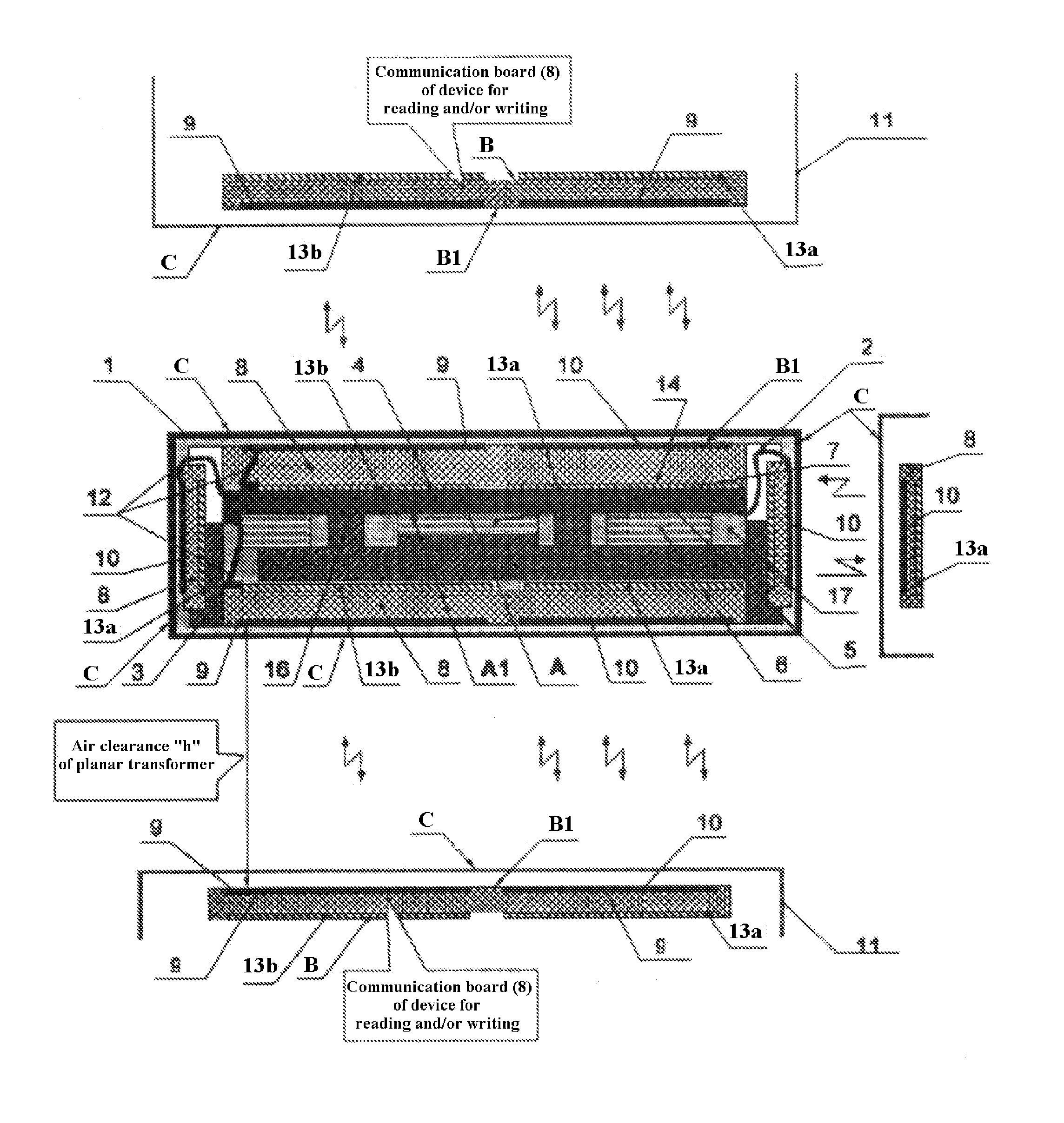
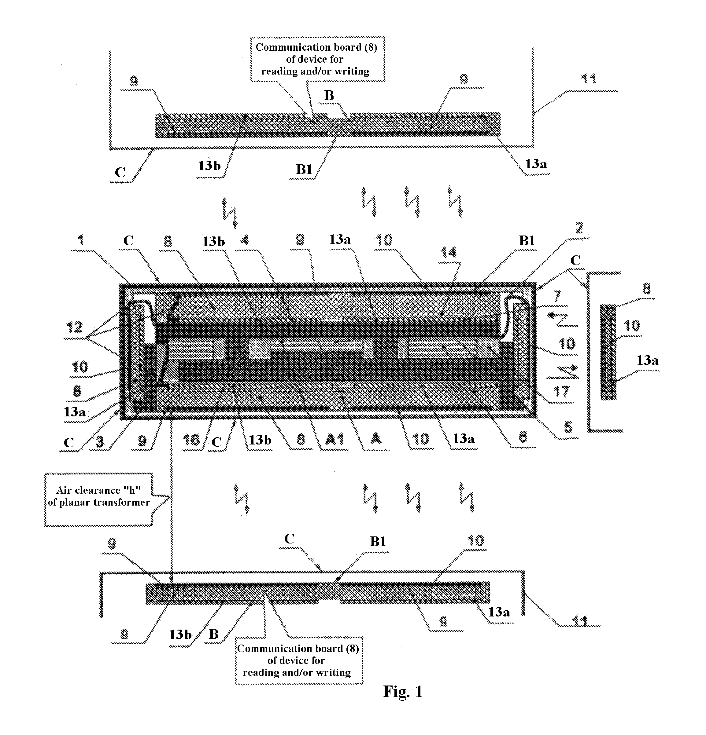
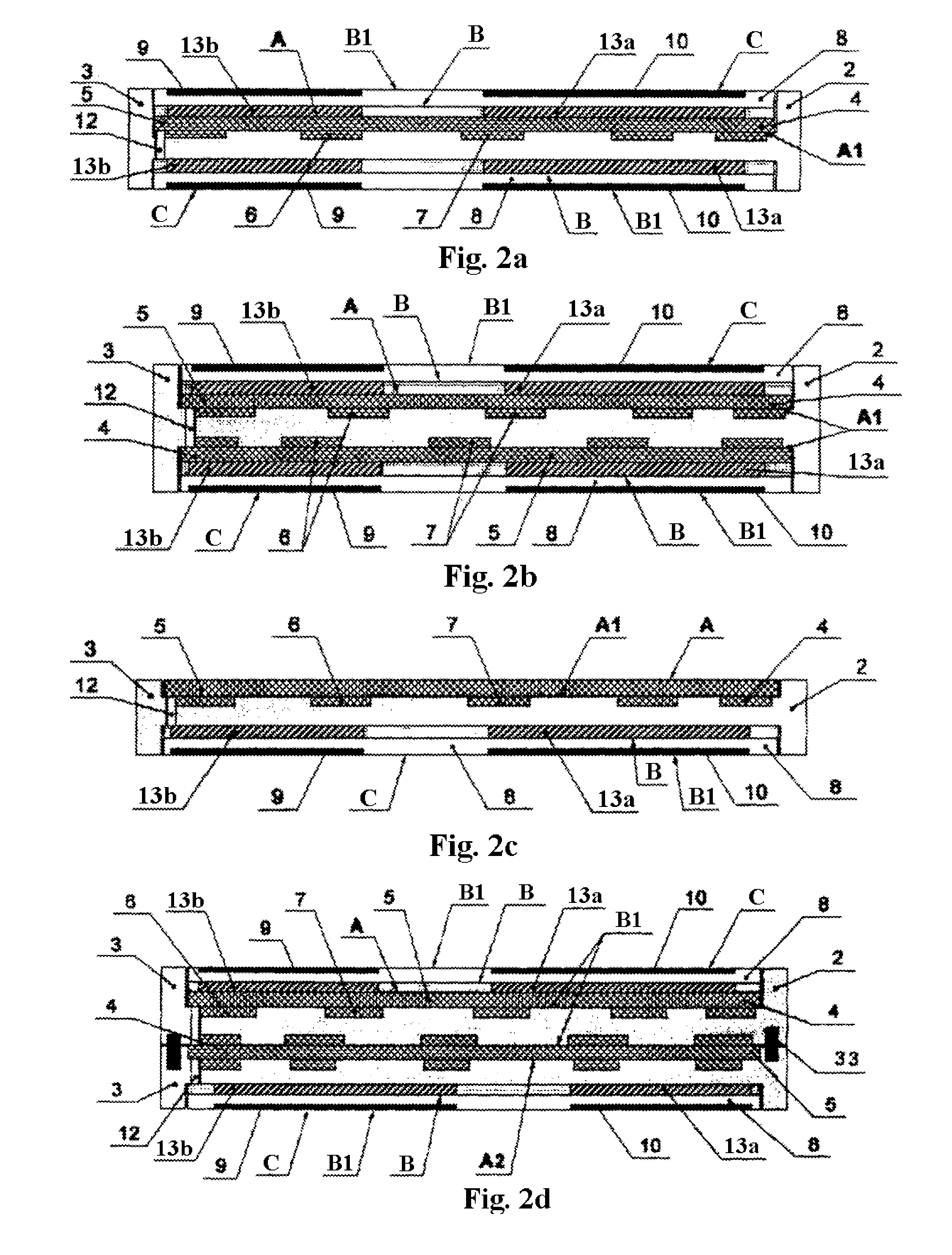
[0039]The SPI device comprises a protective casing (1) of a unit (2) for storing and processing information (an SPI unit) comprising a base (3), a logic board (4) provided with a switching board (5) having switching layers, the switching layers including surface layers A (no components are provided) and mounting layers A1, A2 (components are provided), wherein microelectronic units (6), semiconductor devices and other radio components (7) combined into an electrical circuit are mounted on A1 layers. Furthermore, the SPI unit comprises a communication board (8) provided with switching layers comprising windings of communication coils (9, 10), wherein the communication board comprises two switching surface layers B and B1, and outer windings of communication coils (9, 10) are provided on the surface switching layer B1. Communication coils (9, 10) of the communication boards (8) are secondary coils of a planar transformer, the planar trans...


PUM


Abstract

The invention relates to a device for storing and processing information (SPI device) comprising a sealed protective casing produced from conductive non-magnetic material, and a unit for storing and processing information, the unit comprising a base, a logic board, communication boards, magnetic cores and electrical coupling components which are combined into an electrical circuit of the stand-alone unit for storing and processing information, and can be used in the field of radio electronics, computation, informatics, and telecommunications as a portable integrated solid-state device which is provided with a contactless input of electrical energy and information signals from another electrical energy apparatus. An achieved technical result is in wider applicability of the SPI device, increased protection of information, and improved characteristics, such as resistance to environmental impacts, higher operating speed, reliability, and multifunctional performance, improvement of mass-dimensional properties and production processability index.

Description

CROSS-REFERENCE TO RELATED APPLICATION[0001]This application claims the benefits from the International Application PCT / RU2009 / 000599 filed on Nov. 2, 2009. The content of this application is hereby incorporated by reference in its entirety.TECHNICAL FIELD[0002]The invention relates to radio electronics, computation, informatics, and telecommunications and can be used as a portable integrated solid-state device which is provided with a contactless input of electrical energy and information signals from another electrical energy apparatus. The device is intended for storing and processing short-term, long-term, private, corporative, and other information data.BACKGROUND OF THE INVENTION[0003]An achieved technical result is in wider applicability of the SPI device, increased protection of information, and improved characteristics, such as resistance to environmental impacts, higher operating speed, reliability, and multifunctional performance, improvement of mass-dimensional propertie...

Claims


Application Information

Patent Timeline
Patent Type & Authority Applications(United States)
IPC IPC(8): H05K7/00G06K19/06
CPCH01L23/552G06K19/07749H01L2924/0002H01L2924/00
Inventor LEONTIEV, VLADIMIR VASILIEVICHLEONTIEV, SERGEY VLADIMIROVICH
Owner LEONTIEV VLADIMIR VASILIEVICH
Why Eureka
Try Eureka