Top drain ldmos

a technology of ldmos and top drain, which is applied in the direction of semiconductor power devices, electrical equipment, basic electric elements, etc., can solve the problems of source inductance, source inductance, and the challenges of conventional technologies to further reduce the source inductance of semiconductor power devices including fet, mosfet and jfet devices, etc., to reduce cell pitch and reduce die costs.

Active Publication Date: 2012-11-01
ALPHA & OMEGA SEMICON INC
View PDF8 Cites 33 Cited by
  • Summary
  • Abstract
  • Description
  • Claims
  • Application Information

AI Technical Summary

Benefits of technology

[0012]It is therefore an aspect of the present invention to provide a new and improved top-drain lateral diffusion MOS (TD-LDMOS) semiconductor power device implemented with a trench source-body interconnect extending from the top surface through the body region down to the bottom source electrode. The device configuration has a reduced cell pitch for reducing die costs such that the above discussed technical difficulties and limitations can be overcome.

Problems solved by technology

Conventional technologies to further reduce the source inductance for semiconductor power devices including the source inductance in FET, MOSFET and JFET devices are challenged by several technical difficulties and limitations.
Specifically, there are technical challenges faced by those of ordinary skill in the art to reduce the source inductance.
There are difficulties in such approaches due to the facts that typical vertical semiconductor power devices is arranged to place the drain electrode on the substrate.
However, in these disclosures, the devices use a single metal over the source / body contact regions and gate shield regions, which is thick (3 um or more) then due to its thickness it will have higher capacitance from the source metal to N-drift drain, more stress on the gate and also larger spacing to drain metal, thus increases the cell pitch.
However, using two metals adds cost since it needs two extra masks—one for via and the other for top metal.
These configurations generally form the P+ sinker through top down diffusion resulting in large cell pitch due to the significant lateral diffusions of the deep sinker used to connect the top source down to the highly doped substrate, which increases the overall size of the cell over the horizontal plane.
A large cell pitch also increases the device costs due to a larger size of the device and a larger size package.
Furthermore, reducing the cell pitch of these prior art bottom-source devices results in shifts in the electrical performance of the device.
For example, bringing the diffused sinker (which is p+ in doping) closer to the source side of the gate in FIG. 1A will result in a higher threshold voltage since the lateral diffusion of the diffused p+ sinker used to connect the top source to the bottom substrate will encroach in the channel region under the gate, which is also p-type, increase the doping concentration in the channel and hence, increase the threshold voltage, which is an undesirable result.
However, significant lateral diffusions of the deep P+ sinker used to connect the top source down to the highly doped substrate occupies greater space thus limiting further reduction and shrinking of the cell pitches.

Method used


Image

  • Top drain ldmos
  • Top drain ldmos
  • Top drain ldmos

Examples


Embodiment Construction

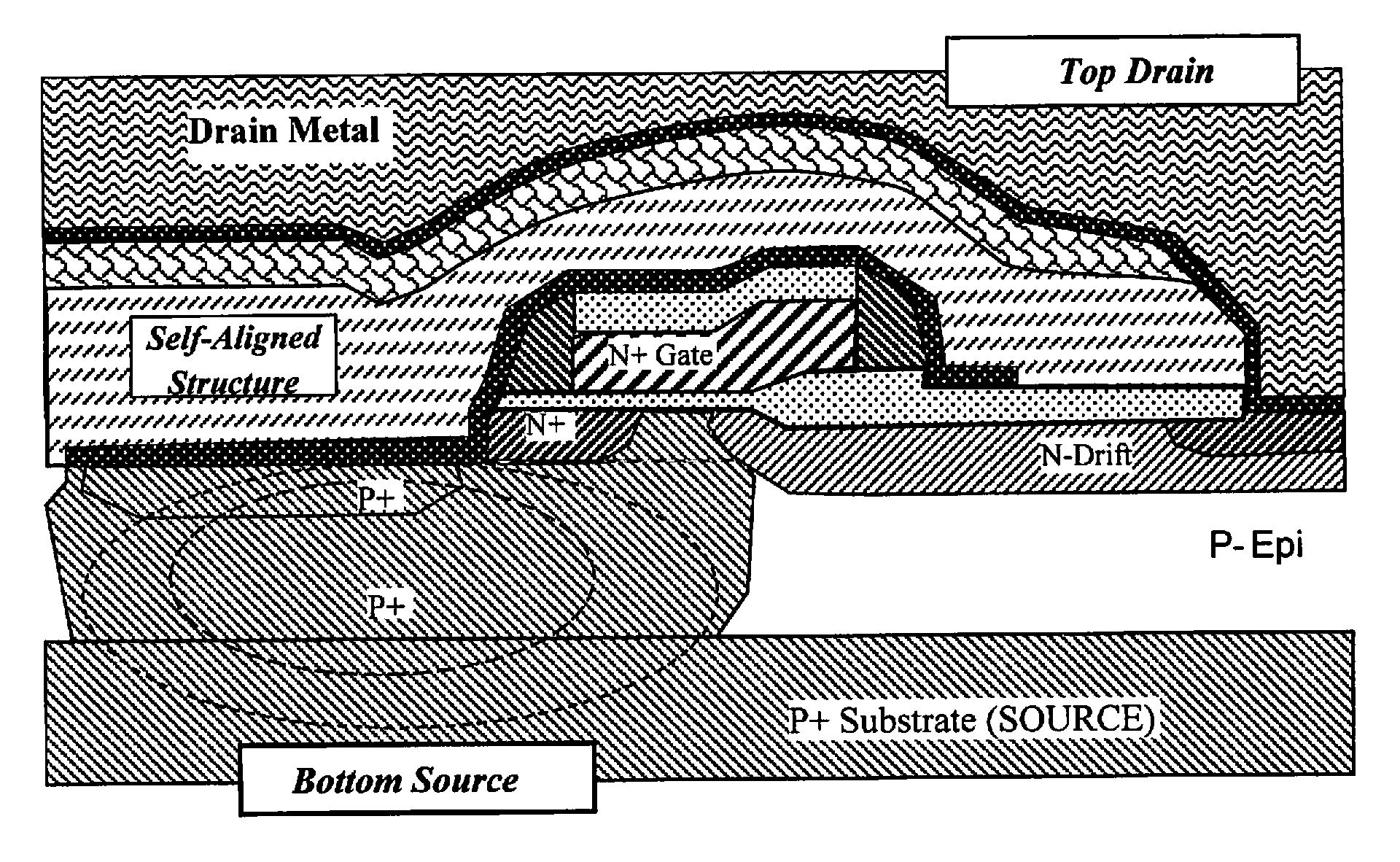
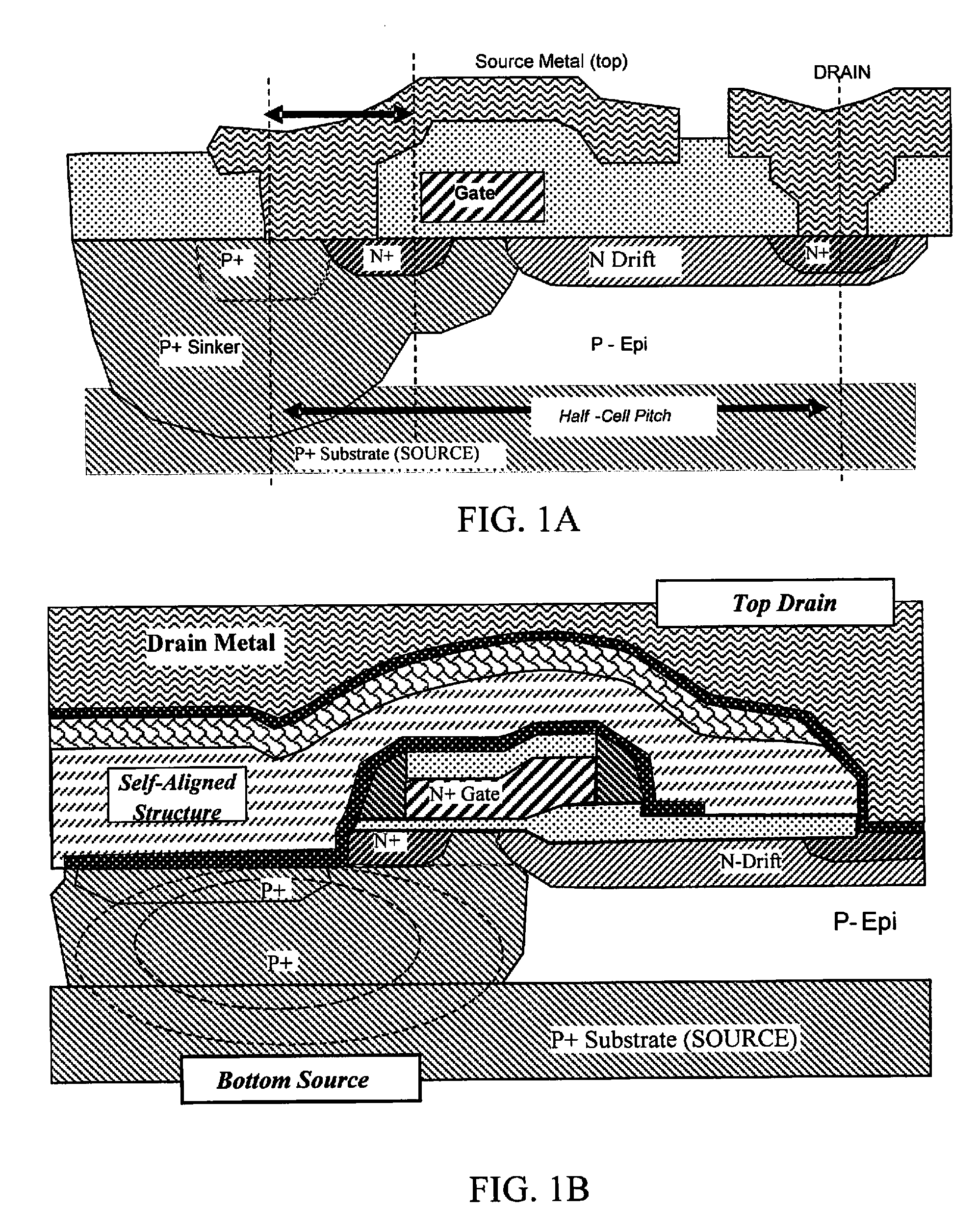
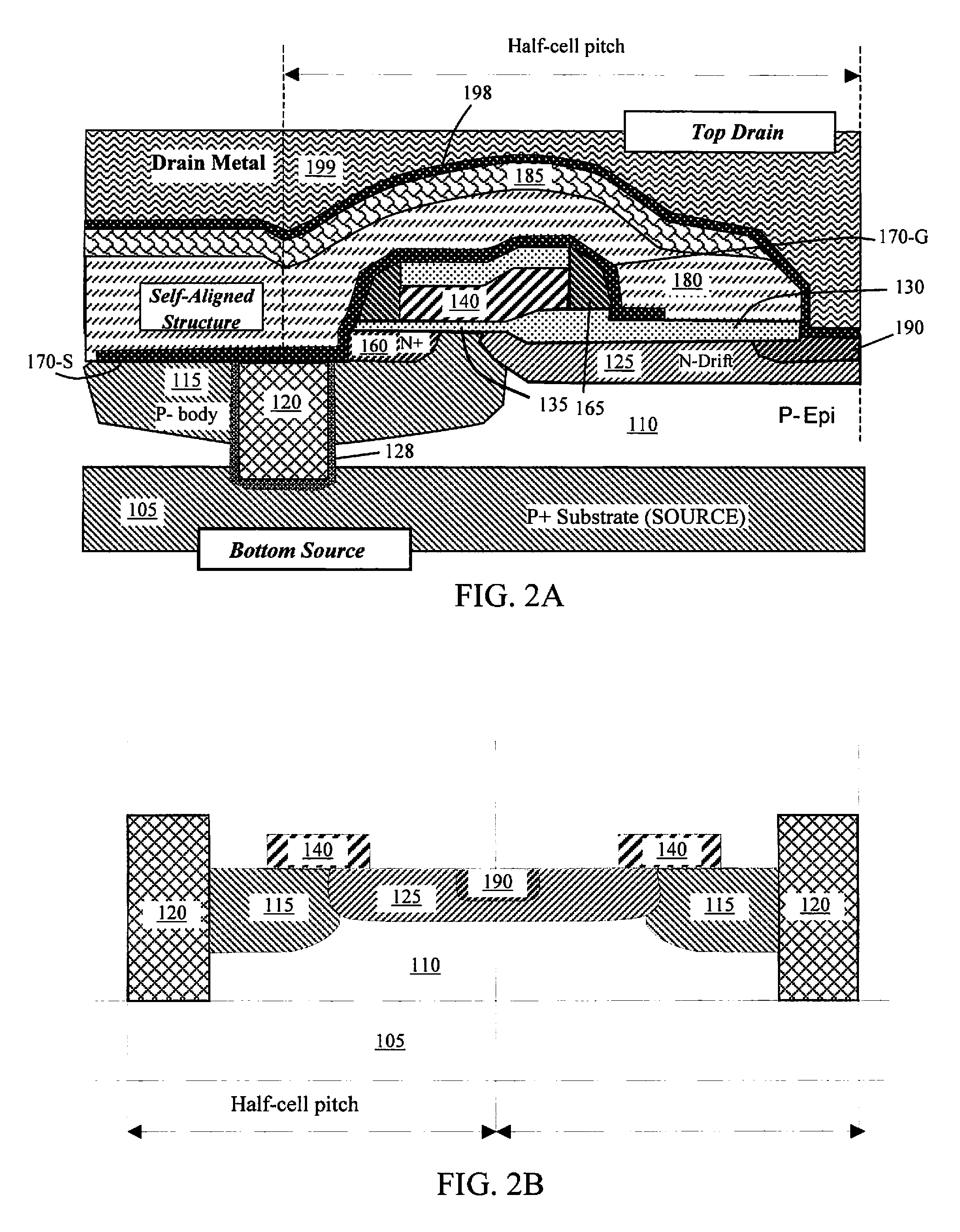
[0027]Referring to FIG. 2A for a cross sectional view of an N-channel inverted top drain and ground-source trenched FET device with a top drain and a bottom source of this invention. The inverted top-drain ground-source N-channel FET device is supported on a P+ substrate 105 functioning as a bottom source electrode. Alternatively, a P-channel device may be formed over an N+ Si substrate. A layer of P− epitaxial layer 110 is supported on top of the substrate 105. The substrate is configured with an active cell area and a termination area typically disposed on the peripheral of the substrate. A deep trench 120 with a high aspect ratio is opened through the epitaxial layer 110 and extending downwardly to the substrate 105. Selective epitaxial growth (SEG) of silicon or SEG of silicon-germanium (SiGe) with a heavily P doped P++ is performed to fill the deep trench 120 forming a self-aligned source / body contact functioning as an ultra-low resistive local interconnect from source to body ...


PUM


Abstract

In an embodiment, this invention discloses a top-drain lateral diffusion metal oxide field effect semiconductor (TD-LDMOS) device supported on a semiconductor substrate. The TD-LDMOS includes a source electrode disposed on a bottom surface of the semiconductor substrate. The TD-LDMOS further includes a source region and a drain region disposed on two opposite sides of a planar gate disposed on a top surface of the semiconductor substrate wherein the source region is encompassed in a body region constituting a drift region as a lateral current channel between the source region and drain region under the planar gate. The TD-LDMOS further includes at least a trench filled with a conductive material and extending vertically from the body region near the top surface downwardly to electrically contact the source electrode disposed on the bottom surface of the semiconductor substrate.

Description

[0001]This patent application is a Continuation in Part Application of application Ser. No. 13 / 095,539 filed on Apr. 27, 2011 by a common Inventor of this Application. The Disclosures made in the patent application Ser. No. 13 / 095,539 are hereby incorporated by reference.BACKGROUND OF THE INVENTION[0002]1. Field of the Invention[0003]The invention relates generally to the semiconductor power devices. More particularly, this invention relates to an inverted grounded source lateral diffusion metal oxide semiconductor field effect transistor (LDMOSFET) structure and manufacturing method.[0004]2. Description of the Prior Art[0005]Conventional technologies to further reduce the source inductance for semiconductor power devices including the source inductance in FET, MOSFET and JFET devices are challenged by several technical difficulties and limitations. Specifically, there are technical challenges faced by those of ordinary skill in the art to reduce the source inductance. Meanwhile, th...

Claims


Application Information

Patent Timeline
Patent Type & Authority Applications(United States)
IPC IPC(8): H01L29/78H01L21/336
CPCH01L29/4175H01L29/41766H01L29/456H01L29/402H01L29/7835H01L29/0692H01L29/1083H01L29/66659H01L29/161H01L29/66681
Inventor MALLIKARJUNASWAMY, SHEKARCHEN, JOHNHU, YONGZHONG
Owner ALPHA & OMEGA SEMICON INC
Why Eureka
Try Eureka