Method for manufacturing semiconductor device

a manufacturing method and semiconductor technology, applied in semiconductor/solid-state device manufacturing, basic electric elements, electric devices, etc., can solve the problems of defective filling (voids), environmental harm, and restricted filling method in the sti for manufacturing semiconductor devices

Inactive Publication Date: 2012-11-01
LONGITUDE LICENSING LTD
View PDF1 Cites 39 Cited by
  • Summary
  • Abstract
  • Description
  • Claims
  • Application Information

AI Technical Summary

Benefits of technology

[0015]According to one embodiment of the present invention, although the conversion of the flowable silazane compound into the first silicon oxide film by heat treatment is accompanied with volume shrinkage, a space for vertical film shrinkage can be ensure by overfilling the flowable silazane compound up to a level higher than the upper surface of the silicon nitride mask film, and thus it is possible to prevent the first silicon oxide from being porous.
[0016]The present invention uses a flowable silazane compound, and thus does not cause dehydration during conversion into the first silicon oxide, which might otherwise occur in conventional methods using flowable silanols. Therefore, volumetric shrinkage of the film is small, and the combination of overfill may prevent the first silicon oxide from being porous.

Problems solved by technology

A filling method in the STI for manufacture of semiconductor devices tends to be restricted by a high aspect ratio caused by miniaturization, and defective fill (voids) may occur in conventional high-density plasma chemical vapor deposition (HDP-CVD) techniques in forming an isolation region having an isolation width of 100 nm or below by STI.
However, the SOD film uses a solvent, which may cause environmental harm.
Moreover, impurities derived from the applied solvent may remain in the formed film, which may affect on characteristics of semiconductor elements.
The less dense oxide film has a high wet etching rate, which may easily cause to defects in processing.
If the height of the bottom-up fill oxide film is low, the oxide film formed by an HDP-CVD method may have defective fill (voids).
Furthermore, the present inventors have recognized that silicon oxide films formed by conventional flowable CVD methods tend to be porous, which may lead to a high wet etching rate.
For example, wide isolation regions are formed together with narrow isolation regions in a semiconductor device such as a DRAM, however, silicon oxide films formed by a flowable CVD method may suffer from problems of different heights of bottom-up fill oxide films caused by isolation widths.
When wet etching is performed in the final step of a process for forming an isolation region, the etching rapidly progresses when a silicon oxide film is obtained by a flowable CVD method with a high wet etching rate from the oxide film formed by an HDP-CVD method with a low wet etching rate, which may result in non-uniform heights of surfaces of isolation regions.

Method used


Image

  • Method for manufacturing semiconductor device
  • Method for manufacturing semiconductor device
  • Method for manufacturing semiconductor device

Examples


experimental example 1

Investigation of Overfilling Amount

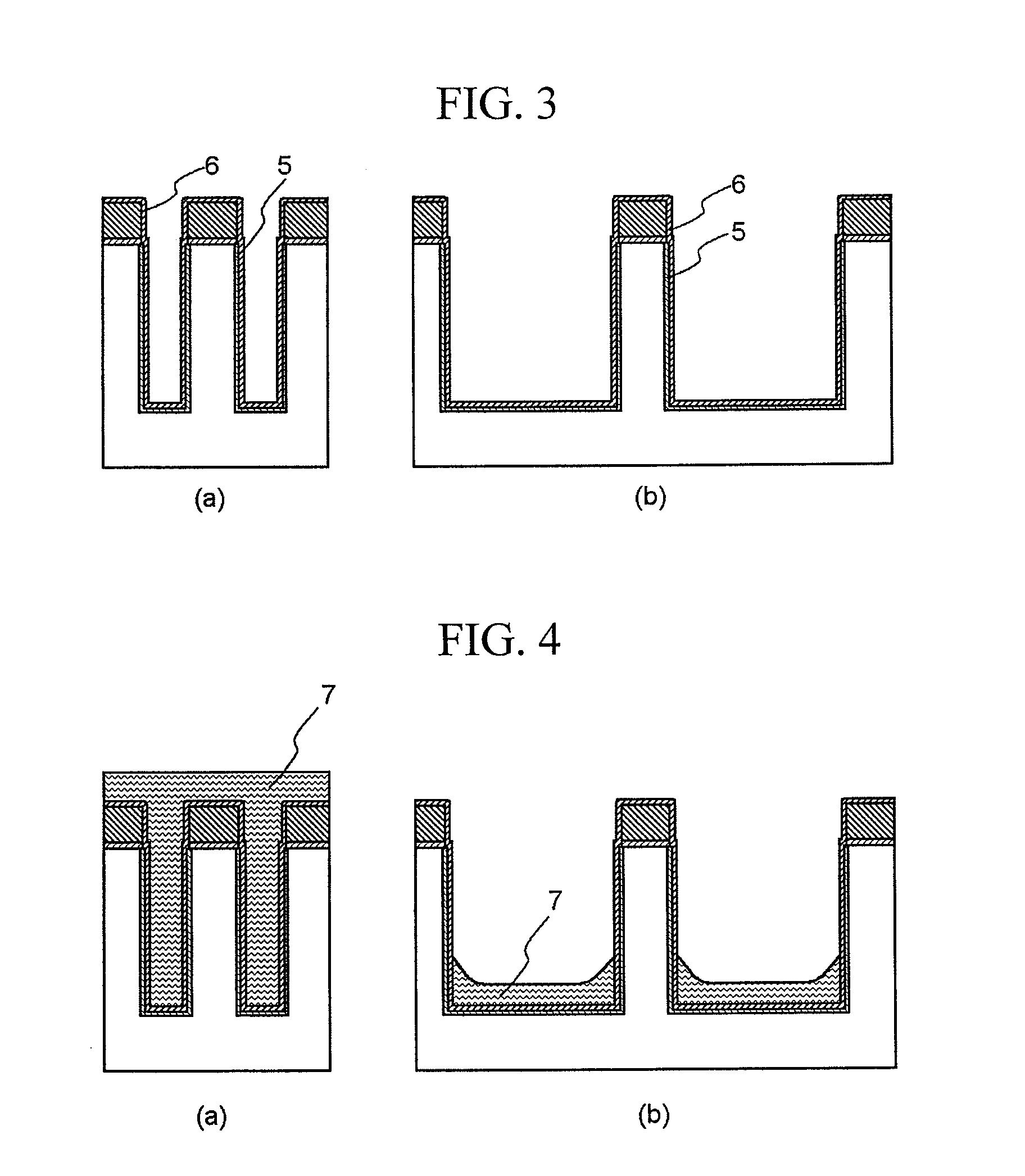
[0041]Now, the aforementioned overfilling amount of the flowable silazane compound film 7 will be explained. The present inventors have performed an experiment in that the flowable silazane compound film 7 is formed by varying the overfilling amount, heat treatment including wet oxidation at 300° C. for 30 minutes, wet oxidation at 800° C. for 60 minutes and nitrogen treatment at 800° C. for 30 minutes is performed to convert the flowable silazane compound film 7 to the first silicon oxide film 8 and simultaneously perform a densification process, a planarization process by CMP is performed as described above, and an etching rate in wet etching is measured. The overfilling amount is set to 0 nm (that is, the height of the upper surface of the flowable silazane compound film 7 over the first isolation trench is the same as the height of the upper surface of the liner silicon nitride film 6 on the silicon nitride mask film 3), 50 nm and 300 nm. Forma...

experimental example 2

Investigation of Heat Treatment Temperature

[0042]The present inventors have studied a heat treatment temperature. The study is conducted on the heat treatment temperature of a high temperature for densification. Test samples are formed by depositing the flowable silazane compound with the overfilling amount of 50 nm and then heat-treating with a first wet oxidation (first stage heat treatment) at 300° C. for 30 minutes, subsequent a second wet oxidation (second stage heat treatment) at temperatures shown in FIG. 11 for 60 minutes, and the third heat treatment for 30 minutes at the temperature same as that of the second wet oxidation under an inert gas atmosphere. In addition, the comparison of the test samples is carried out using a silicon oxide film formed by HD-CVD as a control. The results of the comparison are shown in FIG. 11. As shown in FIG. 11, the wet etching rate becomes lower as the heat treatment temperature rises. As aforementioned, the required thickness of the liner ...


PUM

PropertyMeasurementUnit
heightaaaaaaaaaa
temperatureaaaaaaaaaa

Abstract

Disclosed is a method for manufacturing a semiconductor device, which provides an isolation region in which a dense silicon oxide film is formed in a trench that requires high aspect ratio. The method includes forming an isolation trench using, as an etching mask, a nitride mask film formed on a substrate, forming a liner nitride film in the isolation trench, depositing a flowable silazane compound by a CVD method such that the height of the flowable silazane compound is higher than the upper surface of the nitride mask film from the upper portion of the trench, performing heat treatment under an oxidizing atmosphere to convert the flowable silazane compound film into a silicon oxide film and simultaneously densifying therefor, and planarizing the silicon oxide film to the height of the upper surface of the nitride mask film.

Description

BACKGROUND OF THE INVENTION[0001]1. Field of the Invention[0002]The present invention relates to a method for manufacturing a semiconductor device, and more particularly, to a method which forms an isolation region with a narrow isolation width on a semiconductor substrate without leaving voids, surface dents or the like. In addition, the present invention relates to a method for simultaneously forming an isolation region with a narrow isolation width and an isolation region with a wide isolation width.[0003]2. Description of the Related Art[0004]When forming a switching element such as a transistor on a semiconductor substrate in a semiconductor device such as a dynamic random access memory (DRAM), an isolation region is formed and a transistor region (active region) is defined in the semiconductor substrate. In recent semiconductor devices, shallow trench isolation (STI) is generally performed to form an isolation region and fill a trench formed in a semiconductor substrate with a...

Claims


Application Information

Patent Timeline
Patent Type & Authority Applications(United States)
IPC IPC(8): H01L21/762
CPCH01L21/76224
Inventor MIYAHARA, JIROWU, NAN
Owner LONGITUDE LICENSING LTD
Why Eureka
Try Eureka