Plasmonic and photonic resonator structures and methods for large electromagnetic field enhancements

a plasmonic and plasmonic resonator technology, applied in the direction of instruments, optical waveguide light guides, optical elements, etc., can solve the problems of difficult control of the excitation efficiency of individual nanoparticles, small optical power can be coupled to these structures, and the conventional spr sensor system is usually large and bulky. achieve the effect of reducing the transmission of ligh

Inactive Publication Date: 2012-11-08
GEORGIA TECH RES CORP
View PDF16 Cites 56 Cited by
  • Summary
  • Abstract
  • Description
  • Claims
  • Application Information

AI Technical Summary

Benefits of technology

[0016]According to another exemplary embodiment of the present invention, the plasmonic nanoparticle reduces a transmission of light through the photonic waveguide at the resonance wavelength of the nanoparticle by at least 10%.

Problems solved by technology

However, conventional SPR sensor systems are usually large and bulky because of the excitation and interrogation mechanism that is mostly done through prism coupling and angle interrogation.
Moreover, owing to the small extinction cross-section of such nanoparticles, efficient excitation of individual nanoparticles in a controlled manner is challenging.
However, in spite of the large increase in the absorption and scattering cross section of the molecules attached to those nanoparticles, still only a small portion of the optical power can be coupled to these structures.

Method used


Image

  • Plasmonic and photonic resonator structures and methods for large electromagnetic field enhancements
  • Plasmonic and photonic resonator structures and methods for large electromagnetic field enhancements
  • Plasmonic and photonic resonator structures and methods for large electromagnetic field enhancements

Examples


example 1

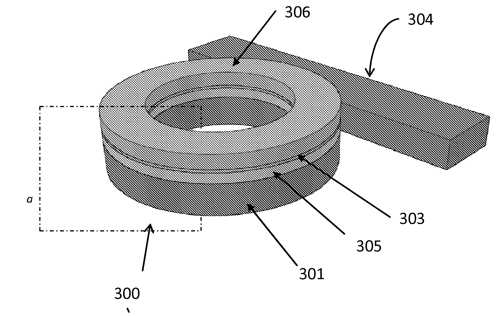
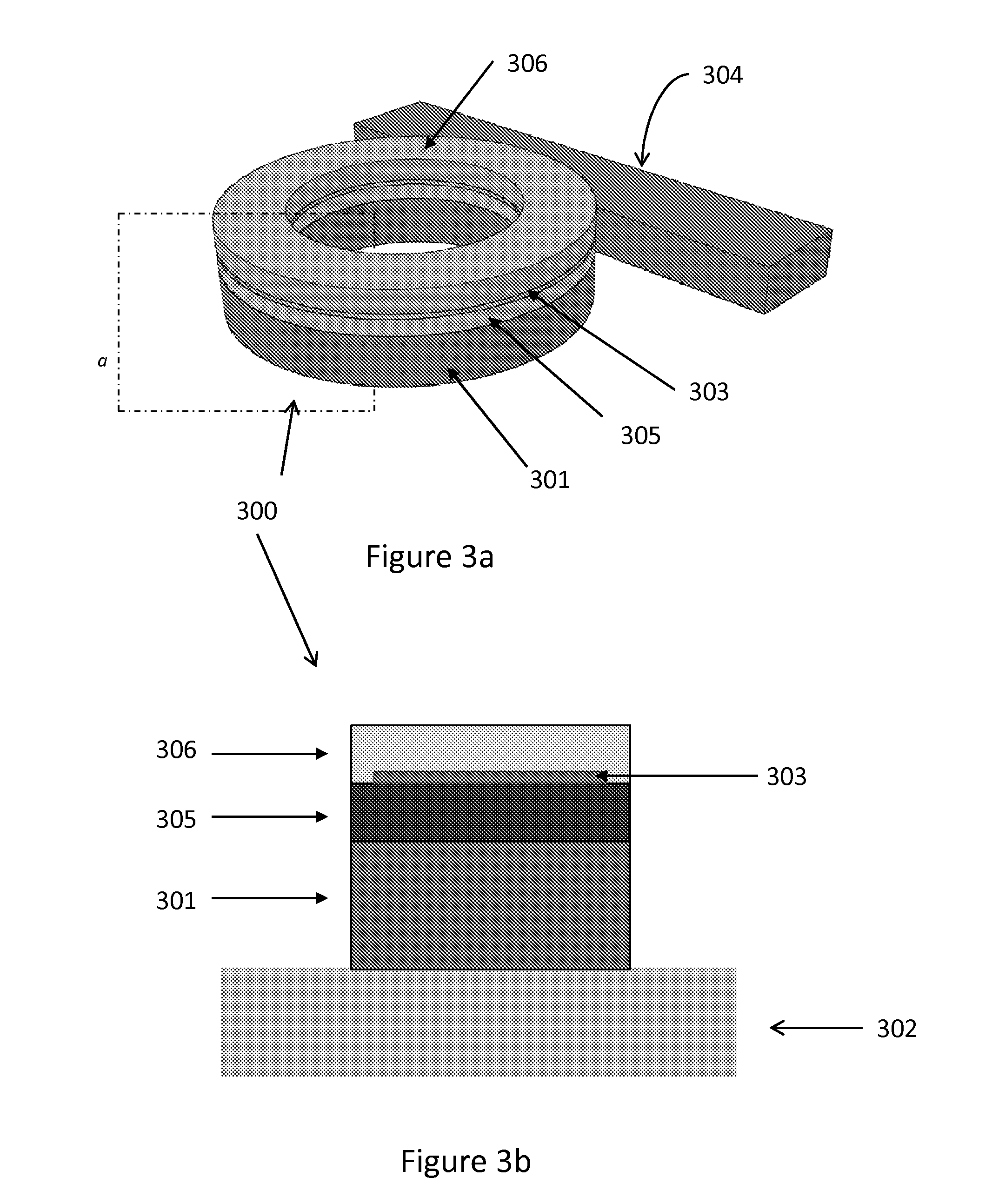
[0083]A biosensor device which used hybrid whispering gallery plasmonic-photonic microring resonator was constructed and theoretically investigated, as shown in FIGS. 3(a) and 3(b), for label-free sensing of biomolecules. The sensor consisted of a silicon nitride (Si3N4) dielectric traveling-wave ring resonator vertically coupled to a thin layer of metallic strip ring resonator on top covered by a porous alumina (p-Al2O3) which served as the sensor interaction medium. In this hybrid resonator, the surface plasmon mode was excited on top of the metallic layer in the porous cladding where the target molecules could efficiently interact with the enhanced electromagnetic field associated with the surface plasmon wave. One of the unique features of this hybrid resonator sensor was the large sensitivity of the surface plasmon waves and the relatively high quality factor Q because of the photonic ring resonator. Sensing of target molecules is performed by transcribing their adsorption to t...

example 2

[0115]The schematic of the hybrid plasmonic-photonic structure consisting of a silicon nitride (Si3N4) ridge waveguide integrated with a gold nanorod on top is shown in FIG. 11. The substrate is silicon dioxide (SiO2). The photonic waveguide with a cross section of (wxh) supports a transverse electric (TE-like) mode over a spectral range that covers the resonance of the plasmonic resonator. The ridge waveguide carries the light and the evanescent tail of the guided mode excites the plasmonic resonatormode. The plasmonic resonatoris assumed to be a gold nanorod with dimensions of (d1×d2×t), where t is the thickness of the gold nanorod. The radius of curvature of the nanorods is assumed to be half of its width, i.e., (d2 / 2). Although we have considered a gold nanorod as the plasmonic resonator, other types of nanoparticles can also be used in the same hybrid structure, and the design, analysis, and implementation will follow the same procedure. Silicon nitride is considered as the mat...

example 3

[0120]The resonance wavelength of the hybrid waveguide plasmonic resonator can be changed by varying the size of the nanoparticle on the surface of a photonic waveguide. Two devices were prepared using standard lithographic techniques. A nanoparticle was placed on the surface of each waveguide, and a broadband light source covering wavelength range of 500 nm to 1700 nm was made to pass through the waveguide with a power spectral density of −54 dBm / nm. The detection was done with only 1 second integration time. These results are shown in Table 2.

TABLE 2WaveguideNanoparticlewidth (nm)dimension (nm)λ0 (nm)Device 1864142 × 56 × 27839Device 2855120 × 56 × 27734


PUM


Abstract

Devices for producing localized surface plasmon resonances are described having a plasmonic resonator and a photonic structure electromagnetically coupled to the plasmonic resonator. The device can include a hybrid photonic plasmonic resonator that contains plasmonic and photonic resonators, and are optionally coupled to a photonic waveguide, or a plasmonic resonator coupled directly to a photonic waveguide. The plasmonic resonator can be one or more nanoparticles. The devices can produce substantial increases in coupling efficiencies and sensitivity for use in several applications, including SERS and refractive index sensing.

Description

CROSS-REFERENCE TO RELATED APPLICATION[0001]The present application claims the benefit of U.S. Provisional Patent Application Ser. No. 61 / 483,731, filed on May 8, 2011, and entitled “Plasmonic and Photonic Resonator Structures and Method for Large Electromagnetic Field Enhancements,” which is hereby incorporated by reference in its entirety as if fully set forth below.TECHNICAL FIELD[0002]The various embodiments of the present invention relate generally to devices having photonic and plasmonic structures, and more particularly to hybrid plasmonic photonic resonators, plasmonic resonators on waveguides and photonic resonators, methods of using same, and apparatus containing same.BACKGROUND[0003]Label-free optical sensing is of great recent interest, especially in biomedical research for sensing biomolecules or monitoring binding kinetics. In this technique, the target molecules need not be labeled, and their existence is directly sensed typically through the change of refractive inde...

Claims


Application Information

Patent Timeline
Patent Type & Authority Applications(United States)
IPC IPC(8): G02B6/10B82Y20/00
CPCB82Y20/00G02B6/1226G02B6/1225G02B6/12007
Inventor CHAMANZAR, MAYSAMREZAEFTEKHAR, ALI ASGHARADIBI, ALI
Owner GEORGIA TECH RES CORP
Why Eureka
Try Eureka