
Simplified organic electronic device employing polymeric anode with high work function

a polymer anode, organic technology, applied in the direction of thermoelectric devices, organic semiconductor devices, other domestic articles, etc., can solve the problems of brittleness and bending of indium tin oxide (ito) electrodes that are commonly used in organic light-emitting diodes and organic solar cells, and the inability to apply flexible devices, etc., to achieve the effect of simplifying the structure of organic solar cells

Inactive Publication Date: 2012-11-29
POSTECH ACAD IND FOUND
View PDF1 Cites 27 Cited by
  • Summary
  • Abstract
  • Description
  • Claims
  • Application Information

AI Technical Summary

Benefits of technology

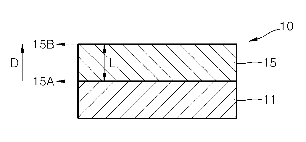
[0009]The present invention provides a simplified electronic device including a flexible electrode with high conductivity and high work function.
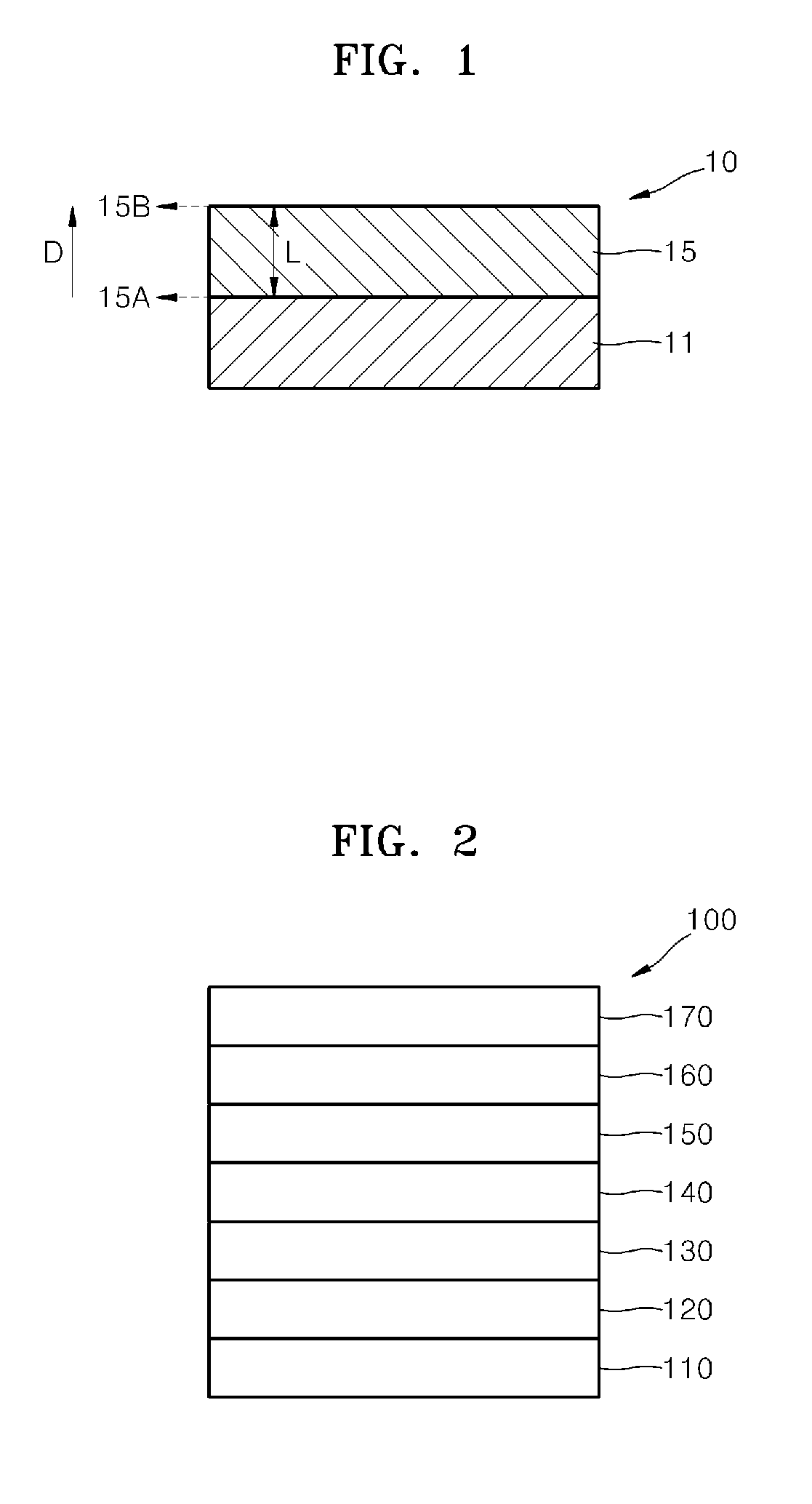
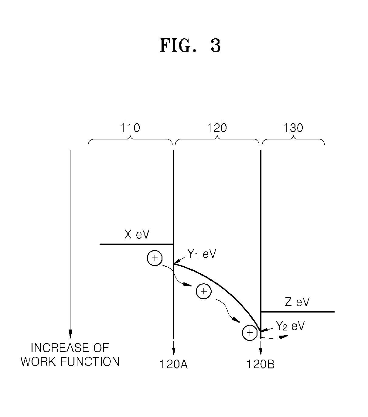
[0021]If the electronic devices are an organic light-emitting device including an emission layer having an ionization potential of 5.0 eV or more greater than a work function of a general indium tin oxide (ITO) electrode, which is in the range of about 4.7 to 4.9 eV, by 0.3 eV or more, a high-work-function and high-conductivity electrode according to the present invention may be used instead of the ITO anode. In this regard, the second surface of the high-work-function and high-conductivity electrode may face the emission layer. In addition, the second surface of the high-work-function and high-conductivity electrode may contact with the emission layer. Alternatively, a hole transport layer may be selectively interposed between the high-work-function and high-conductivity electrode and the emission layer. Here, the second surface of the high-work-function and high-conductivity electrode may contact with the hole transport layer. In general, a hole injection layer and a hole transport layer are interposed between the ITO anode and the emission layer. However, the HIL and / or the HTL may not be formed since the high-work-function and high-conductivity electrode is used. Accordingly, a flexible organic light-emitting display device as well as a flat panel organic light-emitting display device may be manufactured using the high-work-function and high-conductivity electrode, and the structure of the organic light-emitting device may be simplified.
[0022]Meanwhile, if the electronic device is an organic solar cell including a photoactive layer having an ionization potential of 5.0 eV or more greater than a work function of a general ITO electrode by 0.3 eV or more, a high-work-function and high-conductivity electrode according to the present invention may be used instead of the ITO anode. In this regard, the second surface of the high-work-function and high-conductivity electrode may face the photoactive layer. Here, the second surface of the high-work-function and high-conductivity electrode may contact with the photoactive layer. In general, a hole extraction layer is interposed between the ITO anode and the photoactive layer. However, the hole extraction layer may not be formed since the high-work-function and high-conductivity electrode is used. Accordingly, a flexible organic solar cell as well as a flat panel solar cell may be manufactured using the high-work-function and high-conductivity electrode, and the structure of the organic solar cell may be simplified.

Problems solved by technology

The cost of indium tin oxide (ITO) electrodes that are commonly used in organic light-emitting diodes and organic solar cells has continued to increase due to exhaustion of indium, and the ITO is brittle and liable to break upon impact or bending.
Thus, ITO cannot be applied to flexible devices.
Although research into electrodes for replacing the ITO has been conducted, developed electrodes do not have sufficient work function.
However, this structure increases the amount of materials and manufacturing costs for preparing electronic devices.

Method used


Image

  • Simplified organic electronic device employing polymeric anode with high work function
  • Simplified organic electronic device employing polymeric anode with high work function
  • Simplified organic electronic device employing polymeric anode with high work function

Examples


example 1

Preparation of High-Work-Function and High-Conductivity Electrode (I)

[0187]A composition for forming an electrode (100% by weight) including a highly conductive poly(3,4-ethylenedioxythiophene):poly(styrenesulfonate)(PEDOT:PSS) solution having a conductivity of 0.3 S / cm (PH500 manufactured by H.C. Starck GmbH, wherein the content of PSS per 1 part by weight of PEDOT was 2.5 parts by weight), a Polymer 100 solution (prepared by dispersing Polymer 100 represented by the following formula in a mixture of water and alcohol (water:alcohol=4.5:5.5(v / v)) to a 5% by weight, Aldrich Co.) and 5% by weight of dimethylsulfoxide (DMSO) was prepared. In this regard, the ratio of the PEDOT:PSS solution and the Polymer 100 solution was adjusted such that the content (solid content) of Polymer 100 per 1 part by weight of the PEDOT was 1.0 part by weight. A thin film having a thickness of 100 nm and formed using the composition for forming an electrode had a conductivity of 125 S / cm.

[0188]In Polymer ...

example 2

Preparation of OLED

[0207]Electrode 1, as an anode, was formed on the PET substrate according to Example 1, and then a NPB HTL having a thickness of 20 nm, a Bebq2:C545T EML having a thickness of 30 nm, wherein the content of C545T was 1.5% by weight, a Bebq2 ETL having a thickness of 20 nm, a Liq ETL having a thickness of 1 nm, and an Al cathode having a thickness of 130 nm were sequentially formed on the second surface of Electrode 1 by vacuum deposition to prepare OLED 1. OLEDs 2 to 4 were prepared in the same manner as in the preparation of OLED 1 respectively using Electrodes 2 to 4 instead of Electrode 1.

example 3

Preparation of High-Work-Function and High-Conductivity Electrode (II)

[0214]A composition for forming an electrode (100% by weight) including a highly conductive poly(3,4-ethylenedioxythiophene):poly(styrenesulfonate)(PEDOT:PSS) solution having a conductivity of 0.3 S / cm (CLEVIOS™ PH500 manufactured by Heraeus GmbH. & Co (Formerly, H. C. Starck GmbH)), wherein the content of PSS per 1 part by weight of PEDOT was 2.5 parts by weight), 2% by weight of 3,3,3-trifluoropropyl)trichlorosilane (CF3CH2CH2SiCl3), as a fluorinated oligomer, (manufactured by Aldrich Co.), and 5% by weight of dimethylsulfoxide (DMSO), was prepared. The composition for forming an electrode was spin-coated on a PET substrate and heat-treated at 150° C. for 30 minutes to form Electrode 5 having a thickness of 100 nm. Electrode 5 had a conductivity of 350 S / cm and a work function of 5.25 eV.


PUM

PropertyMeasurementUnit
Lengthaaaaaaaaaa
Electrical conductivityaaaaaaaaaa
Energyaaaaaaaaaa

Abstract

An electronic device employing a polymeric anode with high work function.

Description

CROSS-REFERENCE TO RELATED PATENT APPLICATION[0001]This application claims the benefit of Korean Patent Application No. 10-2011-0050845, filed on May 27, 2011, in the Korean Intellectual Property Office, the disclosure of which, is incorporated herein in its entirety by reference.BACKGROUND OF THE INVENTION[0002]1. Field of the Invention[0003]The present invention relates to a simplified organic electronic device including a polymeric anode with high work function.[0004]2. Description of the Related Art[0005]Organic light-emitting devices, which are self-emitting devices, have advantages such as a wide viewing angle, excellent contrast, quick response, high brightness, excellent driving voltage characteristics, and can provide multicolored images.[0006]A conventional organic light-emitting device includes an anode, a cathode, and an organic layer interposed between the anode and the cathode. The organic layer may include an electron injection layer (EIL), a hole transport layer (HTL...

Claims


Application Information

Patent Timeline
IPC IPC(8): H01L51/30H01L51/54H01L51/46
CPCH01L51/0545C08G65/007H01L51/5206H01L51/5218H01L29/0669H01L29/1606H01L2251/5338H01L2251/5346H01L2251/5369H01L2251/55Y02E10/549C08L27/18H01L51/105C08L25/18C08L65/00Y10S428/917H10K10/466H10K10/84H10K50/818H10K2101/80H10K2102/331H10K2102/311H10K2101/10H10K50/81H10K2101/00
Inventor LEE, TAE-WOOWOO, SEONG-HOON
Owner POSTECH ACAD IND FOUND
Learn More