Photoelectric conversion device, imaging device and production methods thereof

a technology of photoelectric conversion and imaging device, which is applied in thermoelectric devices, organic semiconductor devices, and nano-informatics. it can solve the problems of reducing the aperture ratio, the photoelectric conversion efficiency is low, and the conventional imaging device called a ccd-type image sensor or a cmos-type image sensor is approaching the limit of its production, so as to achieve high photoelectric conversion efficiency

Active Publication Date: 2012-12-13
FUJIFILM CORP
View PDF3 Cites 31 Cited by
  • Summary
  • Abstract
  • Description
  • Claims
  • Application Information

AI Technical Summary

Benefits of technology

[0034]According to an exemplary embodiment of the present invention, a fullerene polymer is previously formed in an organic photoelectric conversion layer, so that a high photoelect

Problems solved by technology

However, such an organic photoelectric conversion layer has a problem that in the initial stage of receiving light irradiation, the photoelectric conversion efficiency is low.
In an imaging device for taking a subject image, individual pixels have a photoelectric conversion device, but the conventional imaging device called a CCD-type image sensor or a CMOS-type image sensor is approaching the limit of its production due to microfabrication and facing various problems.
As just described, in the image sensor in the related art, not only a photodiode as a photoelectric conversion device but also, for example, a signal readout circuit and a multilayer wiring associated therewith are formed together on a semiconductor substrate, and as the miniaturization of a pixel proceeds, the region occupied by the signal readout circuit or wiring in one pixel becomes relatively large, raising a problem of “reduction of aperture ratio”, that is, the light-receiving area of the photodiode on one chip being relatively decreased.
The reduction of aperture ratio leads to reduction in sensitivity, and it becomes difficult to take a bright image or a low-noise image.
Ho

Method used


Image

  • Photoelectric conversion device, imaging device and production methods thereof
  • Photoelectric conversion device, imaging device and production methods thereof
  • Photoelectric conversion device, imaging device and production methods thereof

Examples


example 1

Synthesis of Compound 15

[0199]Compound 15 that is one of arylidene compounds was synthesized in accordance with a known method (U.S. Patent Application Publication No. 2005 / 0065351).

(Fabrication of Device)

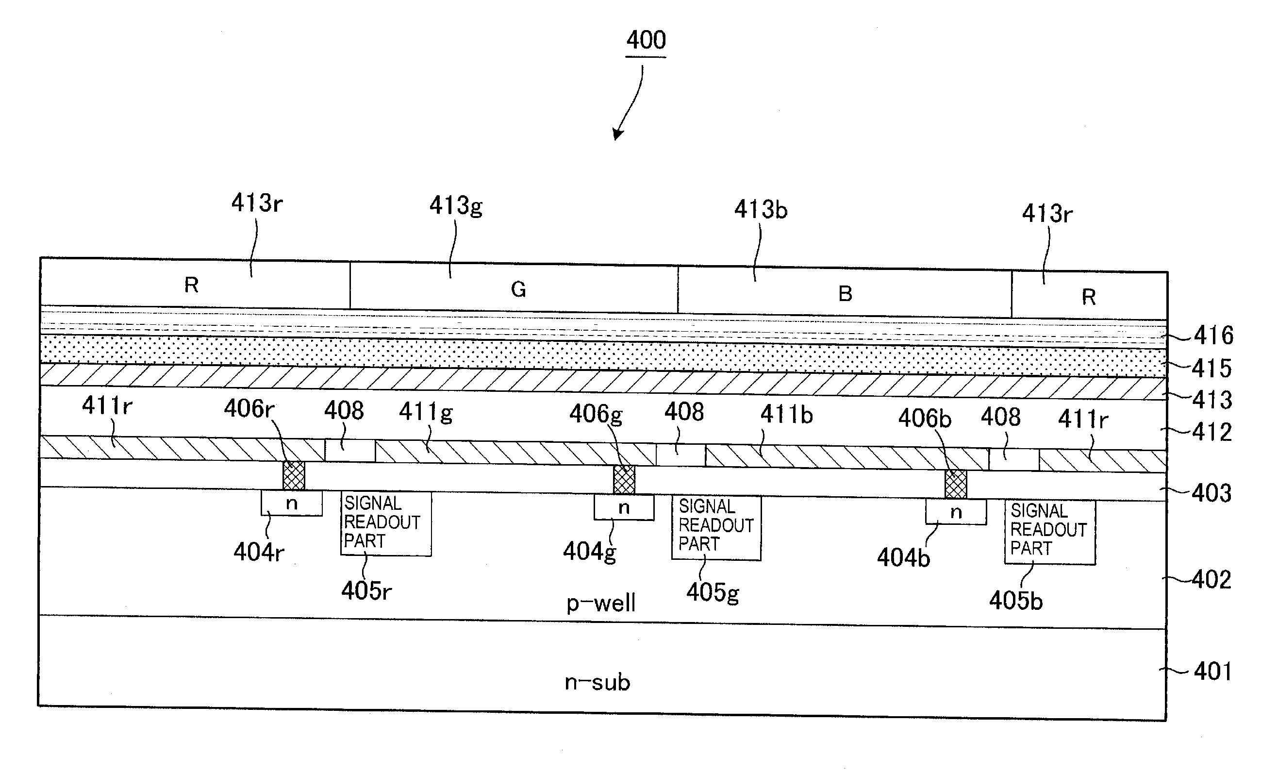
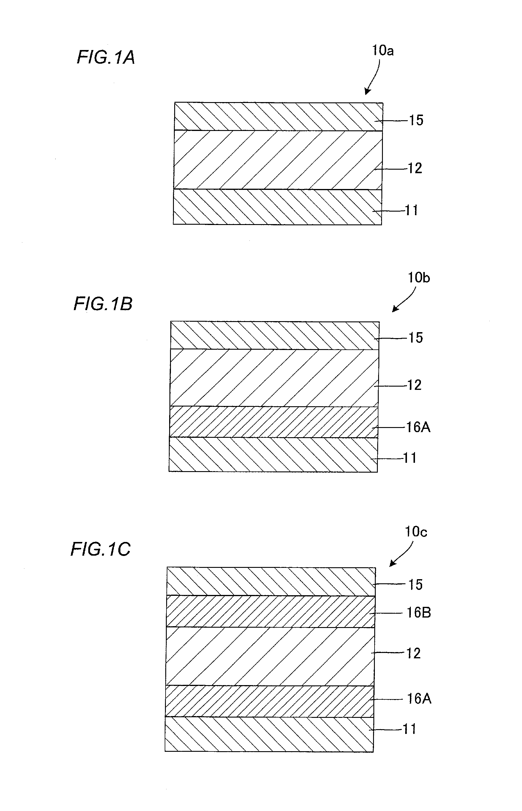
[0200]On a semiconductor substrate having formed therein a CMOS circuit as a signal readout circuit, an amorphous ITO layer was deposited by sputtering to a thickness of 30 nm and patterned by photolithography to allow one pixel to exist for each photodiode (PD) on the semiconductor substrate, thereby forming pixel electrodes, and a layer of an electron blocking material (EB-3) was deposited thereon to a thickness of 100 nm by vacuum heating deposition. Subsequently, a layer of 400 nm in thickness obtained by co-depositing Compound 15 and fullerene (C60) in a ratio of 200 nm and 200 nm in terms of a single layer was deposited thereon by vacuum heating deposition to form a photoelectric conversion layer. Furthermore, an amorphous ITO layer was deposited as the upper electrode by spu...

example 2

Synthesis of Compound 16

[0202]Compound 16 that is one of arylidene compounds was synthesized in accordance with a known method (U.S. Patent Application Publication No. 2005 / 0065351).

(Identification of Compound 16)

[0203]1H NMR (CDCl3) δ: 7.16 (2H, d), 7.30-7.40 (6H, m), 7.42-7.51 (4H, m), 7.60-7.70 (10H, m), 7.90 (1H, s), 8.09 (2H, m), 8.46 (2H, d), 8.55 (2H, d).

(Fabrication of Device)

[0204]A solid-state imaging device was fabricated in the same manner as in Example 1 except for changing Compound 15 in the organic photoelectric conversion layer 12 to Compound 16.

example 3

Synthesis of Compound 17

[0205]Compound 17 was synthesized in accordance with a known method (U.S. Patent Application Publication No. 2005 / 0065351).

(Fabrication of Device)

[0206]A solid-state imaging device was fabricated in the same manner as in Example 1 except for changing Compound 15 in the organic photoelectric conversion layer 12 to Compound 17.


PUM


Abstract

A photoelectric conversion device is provided and includes: a first electrode, a second electrode, and a photoelectric conversion layer between the first and second electrodes, the photoelectric conversion layer containing a mixture of an organic photoelectric conversion dye, a fullerene or a fullerene derivative, and a fullerene polymer; various embodiments of the device, a photosensor, an imaging device, and production methods for these devices.

Description

TECHNICAL FIELD[0001]The present invention relates to a photoelectric conversion device used for solar cells and the like, an imaging device used as an image sensor, and production methods thereof. More specifically, the present invention relates to a photoelectric conversion device having, as an organic photoelectric conversion layer, a mixture of an organic photoelectric conversion dye and a fullerene, an imaging device, and production methods thereof.BACKGROUND ART[0002]A photoelectric conversion device having, as an organic photoelectric conversion layer, a mixture of an organic photoelectric conversion dye and a fullerene, described, for example, in JP-A-2001-7366 is attracting attention. A solar cell that receives sunlight and produces an electric energy is remarkably spreading as an apparatus for producing a clean energy replacing the petroleum energy, and above all, a solar cell having, as an organic photoelectric conversion layer, a mixture of an organic photoelectric conve...

Claims


Application Information

Patent Timeline
IPC IPC(8): H01L51/46H01L51/48
CPCB82Y10/00Y02E10/549H01L27/14632H01L27/14645H01L27/307H01L51/0047H01L51/0051H01L51/0053H01L51/0059H01L51/006H01L51/0065H01L51/0072H01L51/4253H01L2251/308H01L27/1463H10K39/32H10K85/215H10K85/611H10K85/621H10K85/653H10K85/633H10K85/631H10K30/30H10K85/6572H10K2102/103H01L31/10H10K30/00
Inventor YOFU, KATSUYUKISAWAKI, DAIGO
Owner FUJIFILM CORP
Why Eureka
Try Eureka