

Plasma processing apparatus and plasma processing method
- Summary
- Abstract
- Description
- Claims
- Application Information
AI Technical Summary
Benefits of technology
Problems solved by technology
Method used
Image

Examples
first embodiment
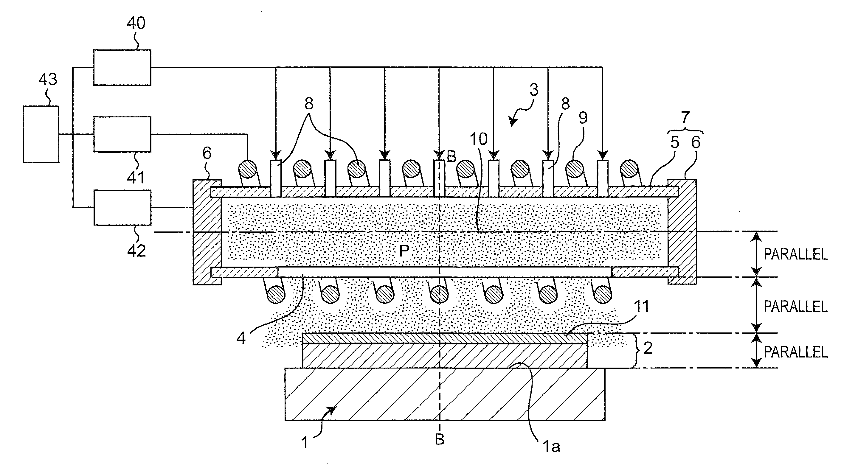
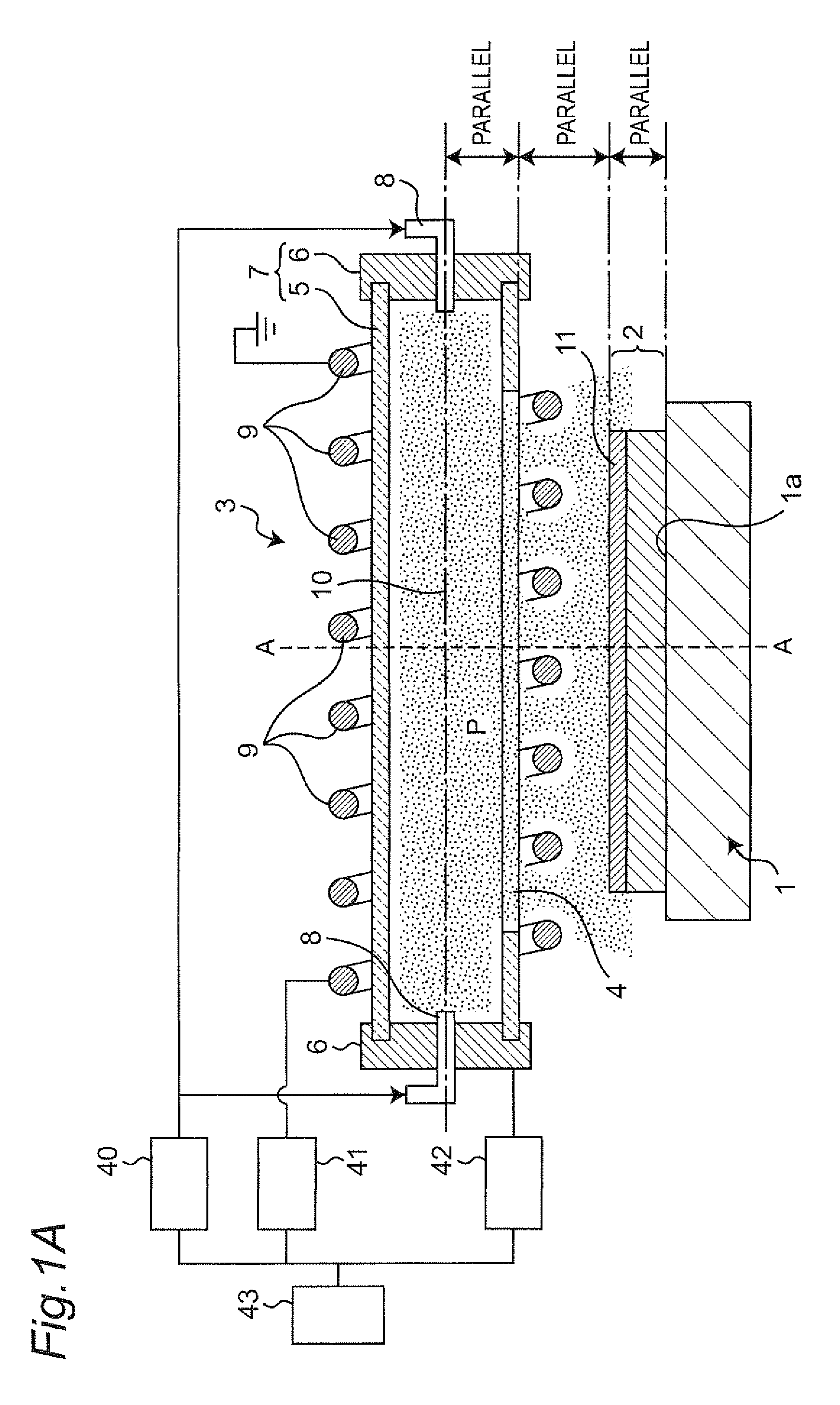
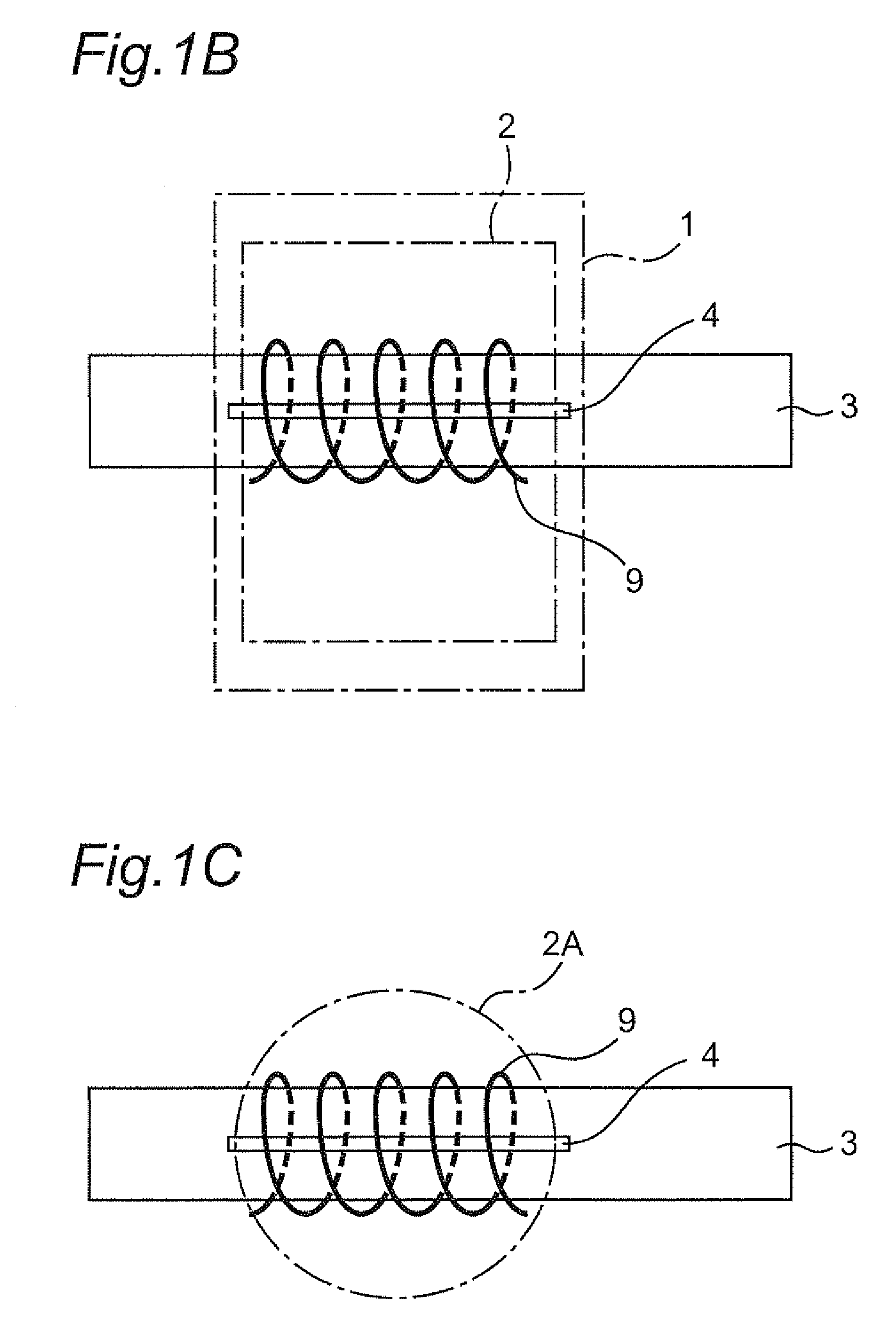
[0110]In the following, with reference to FIGS. 1A to 4, a description will be given of a first embodiment of the present invention.
[0111]FIG. 1A shows the structure of a thermal plasma processing apparatus according to the first embodiment of the present invention. FIG. 1B is a bottom view of the plasma processing apparatus showing the relationship among the plasma processing apparatus according to the first embodiment of the present invention, a quadrilateral base material 2, and a base material placement table 1. FIGS. 1A and 1B are each a cross-sectional view taken along a plane parallel to the longer direction of an inductively coupled plasma torch unit 3, the plane including a center axis 10 of a solenoid coil 9 and being perpendicular to the surface of the base material 2. Further, FIG. 2A is a cross-sectional end view taken along dashed line A-A shown in FIG. 1A. It is to be noted that, in the following description, though the base material 2 is described as being quadrilate...
second embodiment
[0136]In the following, with reference to FIGS. 5A to 6, a description will be given of a second embodiment of the present invention.
[0137]FIG. 5A shows the structure of a thermal plasma processing apparatus according to the second embodiment of the present invention. FIG. 5A is a cross-sectional view taken along a plane parallel to the longer direction of an inductively coupled plasma torch unit 3A, the plane including a center axis 10A of a solenoid coil 9A, and being perpendicular to the surface of the base material 2. Further, FIG. 5B is a bottom view of a plasma processing apparatus showing the relationship among the plasma processing apparatus according to the second embodiment of the present invention shown in 5A, the base material, and the base material placement table. FIG. 6 is a cross-sectional end view taken along dashed line C-C shown in FIG. 5A.
[0138]In FIGS. 5A and 6, the base material 2 is placed on the base material placement face 1a of the base material placement t...
third embodiment
[0149]In the following, with reference to FIGS. 7 and 8, a description will be given of a third embodiment of the present invention.
[0150]FIG. 7 shows the structure of a thermal plasma processing apparatus according to the third embodiment of the present invention. FIG. 7 is a cross-sectional view taken along a plane parallel to the longer direction of an inductively coupled plasma torch unit 3B, the plane including a center axis 10B of a solenoid coil 9B, and being perpendicular to the surface of the base material 2. Further, FIG. 8 is a cross-sectional end view taken along dashed line D-D shown in FIG. 7.
[0151]In FIGS. 7 and 8, the base material 2 is placed on the base material placement face 1a of the base material placement table 1. The inductively coupled plasma torch unit 3B is substantially structured with a cylindrical chamber 7B and a coil case 16, which is an insulating member having a downwardly convex shape whose tip is semicircular.
[0152]The cylindrical chamber 7B is st...
PUM
| Property | Measurement | Unit |
|---|---|---|
| Length | aaaaa | aaaaa |
| Frequency | aaaaa | aaaaa |
| Electromagnetic field | aaaaa | aaaaa |
Abstract
Description
Claims
Application Information